Datasheet Details
| Part number | CY7C2265KV18 |
|---|---|
| Manufacturer | Cypress (Infineon) |
| File Size | 631.21 KB |
| Description | 36-Mbit QDR II+ SRAM Four-Word Burst Architecture |
| Datasheet |
 CY7C2265KV18 Datasheet CY7C2265KV18 Datasheet
|
|
|
Download the CY7C2265KV18 datasheet PDF. This datasheet also covers the CY7C2263KV18 variant, as both devices belong to the same 36-mbit qdr ii+ sram four-word burst architecture family and are provided as variant models within a single manufacturer datasheet.
| Part number | CY7C2265KV18 |
|---|---|
| Manufacturer | Cypress (Infineon) |
| File Size | 631.21 KB |
| Description | 36-Mbit QDR II+ SRAM Four-Word Burst Architecture |
| Datasheet |
CY7C2265KV18 Datasheet
|
|
|
|
| Part Number | Description | Manufacturer |
|---|---|---|
| CY7C225 | 512 x 8 Registered PROM | Cypress |
| CY7C277 | 32K x 8 Reprogrammable Registered PROM | Cypress |
| CY7C008 | 64K/128K x 8/9 Dual-Port Static RAM | Cypress |
| CY7C008V | 3.3V 64K/128K x 8/9 Dual-Port Static RAM | Cypress |
| CY7C009 | 64K/128K x 8/9 Dual-Port Static RAM | Cypress |
| Part Number | Description |
|---|---|
| CY7C2265XV18 | 36-Mbit QDR II+ Xtreme SRAM Four-Word Burst Architecture |
| CY7C2262XV18 | 36-Mbit QDR II+ Xtreme SRAM Two-Word Burst Architecture |
| CY7C2263KV18 | 36-Mbit QDR II+ SRAM Four-Word Burst Architecture |
| CY7C2263XV18 | 36-Mbit QDR II+ Xtreme SRAM Four-Word Burst Architecture |
| CY7C2264XV18 | 36-Mbit QDR II+ Xtreme SRAM Two-Word Burst Architecture |
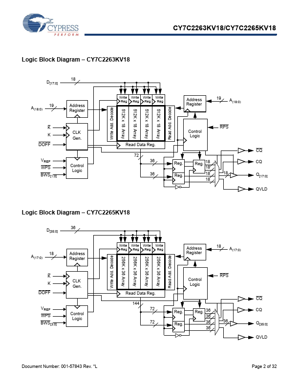
The following content is an automatically extracted verbatim text from the original manufacturer datasheet and is provided for reference purposes only.