Datasheet Details
| Part number | CY7C1514AV18 |
|---|---|
| Manufacturer | Cypress (Infineon) |
| File Size | 690.83 KB |
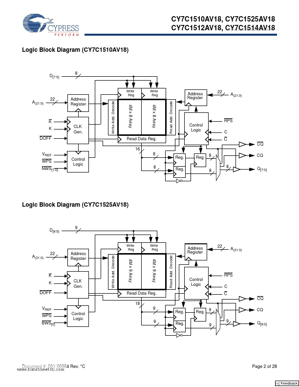
| Description | 72-Mbit QDR-II SRAM 2-Word Burst Architecture |
| Datasheet |
 CY7C1514AV18 Datasheet CY7C1514AV18 Datasheet
|

|
|
Download the CY7C1514AV18 datasheet PDF. This datasheet also covers the CY7C1510AV18 variant, as both devices belong to the same 72-mbit qdr-ii sram 2-word burst architecture family and are provided as variant models within a single manufacturer datasheet.
| Part number | CY7C1514AV18 |
|---|---|
| Manufacturer | Cypress (Infineon) |
| File Size | 690.83 KB |
| Description | 72-Mbit QDR-II SRAM 2-Word Burst Architecture |
| Datasheet |
CY7C1514AV18 Datasheet
|
|
|
|
| Part Number | Description | Manufacturer |
|---|---|---|
| CY7C1518AV18 | 72-Mbit DDR-II SRAM | Cypress |
| CY7C1520AV18 | 72-Mbit DDR-II SRAM | Cypress |
| CY7C1006D | 1-Mbit (256K x 4) Static RAM | Cypress |
| CY7C1011G | 2-Mbit (128K words x 16 bit) Static RAM | Cypress |
| CY7C1041G | 4-Mbit (256K words x 16 bit) Static RAM | Cypress |
| Part Number | Description |
|---|---|
| CY7C1514KV18 | 72-Mbit QDR II SRAM Two-Word Burst Architecture |
| CY7C1514V18 | 1.8V Synchronous Pipelined SRAM |
| CY7C1510AV18 | 72-Mbit QDR-II SRAM 2-Word Burst Architecture |
| CY7C1510V18 | 1.8V Synchronous Pipelined SRAM |
| CY7C1511AV18 | 72-Mbit QDR-II SRAM 4-Word Burst Architecture |