Datasheet Details
| Part number | CY7C1487V25 |
|---|---|
| Manufacturer | Cypress (Infineon) |
| File Size | 1.31 MB |
| Description | 72-Mbit (2M x 36/4M x 18/1M x 72) Flow-Through SRAM |
| Datasheet |
 CY7C1487V25 Datasheet CY7C1487V25 Datasheet
|
|
|
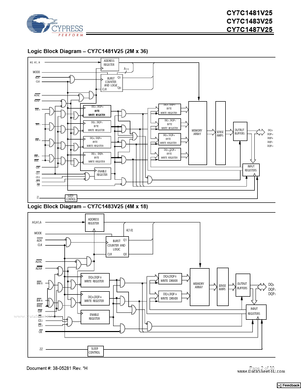
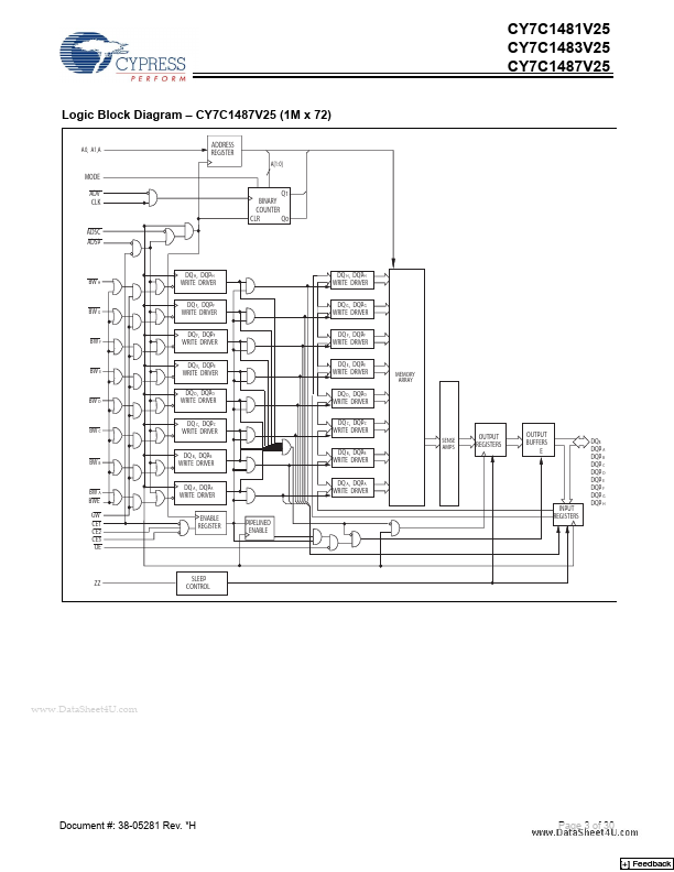
The CY7C1481V25/CY7C1483V25/CY7C1487V25 is a 2.5V, 2M x 36/4M x 18/1M x 72 Synchronous Flow-through SRAM designed to interface with high-speed microprocessors with minimum glue logic.
Maximum access delay from clock rise is 6.5 ns (133-MHz version).
| Part number | CY7C1487V25 |
|---|---|
| Manufacturer | Cypress (Infineon) |
| File Size | 1.31 MB |
| Description | 72-Mbit (2M x 36/4M x 18/1M x 72) Flow-Through SRAM |
| Datasheet |
CY7C1487V25 Datasheet
|
|
|
|
| Part Number | Description | Manufacturer |
|---|---|---|
| CY7C1460SV25 | 36-Mbit (1M x 36/2M x 18) Pipelined SRAM | Cypress |
| CY7C1462SV25 | 36-Mbit (1M x 36/2M x 18) Pipelined SRAM | Cypress |
| CY7C1006D | 1-Mbit (256K x 4) Static RAM | Cypress |
| CY7C1011G | 2-Mbit (128K words x 16 bit) Static RAM | Cypress |
| CY7C1041G | 4-Mbit (256K words x 16 bit) Static RAM | Cypress |
| Part Number | Description |
|---|---|
| CY7C1487V33 | (CY7C1481V33 / CY7C1483V33 / CY7C1487V33) 2M x 36/4M x 18/1M x 72 Flow-Through SRAM |
| CY7C148 | (CY7C148 / CY7C149) 1K x 4 Static RAM |
| CY7C1480BV25 | 72-Mbit (2M x 36/4M x 18/1M x 72) Pipelined Sync SRAM |
| CY7C1480BV33 | (CY7C148xBV33) 72-Mbit (2M x 36/4M x 18/1M x 72) Pipelined Sync SRAM |
| CY7C1480V33 | (CY7C1480V33 / CY7C1482V33 / CY7C1486V33) 72-Mbit (2M x 36/4M x 18/1M x 72) Pipelined Sync SRAM |
The following content is an automatically extracted verbatim text from the original manufacturer datasheet and is provided for reference purposes only.