Download the CY7C1465AV25 datasheet PDF.
This datasheet also covers the CY7C1461AV25 variant, as both devices belong to the same flow-through sram family and are provided as variant models within a single manufacturer datasheet.
Description
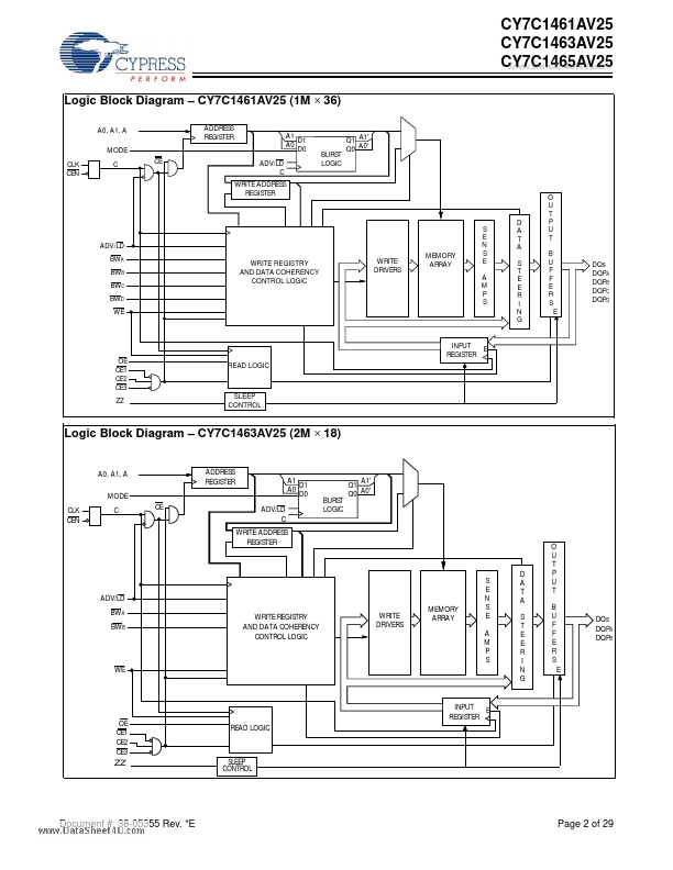
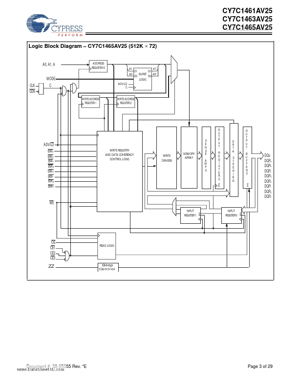
The CY7C1461AV25/CY7C1463AV25/CY7C1465AV25 are 2.5V, 1M × 36/2M × 18/512K × 72 Synchronous Flow-through Burst SRAMs designed specifically to support unlimited true back-to-back Read/Write operations without the insertion of wait states.
Features
- No Bus Latency™ (NoBL™) architecture eliminates dead cycles between write and read cycles.
- Can support up to 133-MHz bus operations with zero wait states.
- Data is transferred on every clock.
- Pin-compatible and functionally equivalent to ZBT™ devices.
- Internally self-timed output buffer control to eliminate the need to use OE.
- Registered inputs for flow-through operation.
- Byte Write capability.
- 2.5V/1.8V I/O power supply.
 CY7C1465AV25 Datasheet