Datasheet Details
| Part number | CY7C1464AV33 |
|---|---|
| Manufacturer | Cypress (Infineon) |
| File Size | 833.98 KB |
| Description | (CY7C146xAV33) 36-Mbit Pipelined SRAM |
| Datasheet |
 CY7C1464AV33 Datasheet CY7C1464AV33 Datasheet
|
|
|
Download the CY7C1464AV33 datasheet PDF. This datasheet also covers the CY7C1460AV33 variant, as both devices belong to the same (cy7c146xav33) 36-mbit pipelined sram family and are provided as variant models within a single manufacturer datasheet.
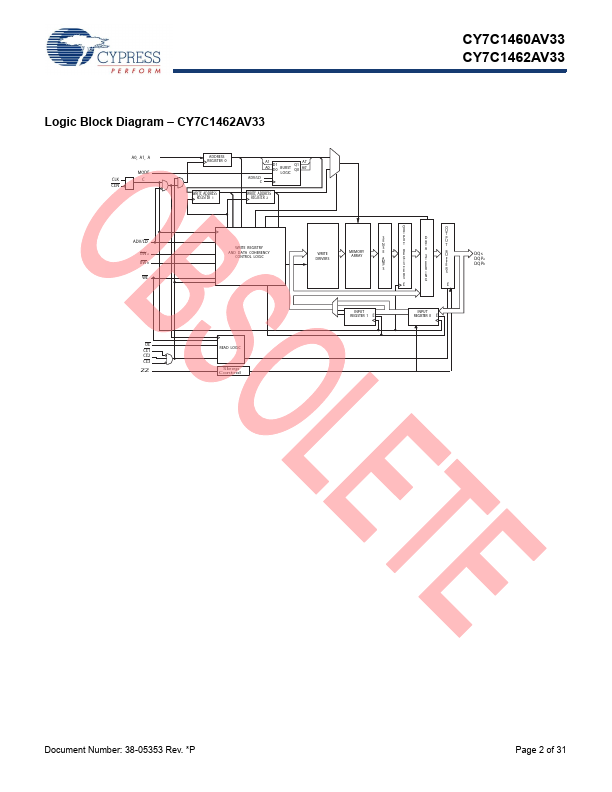
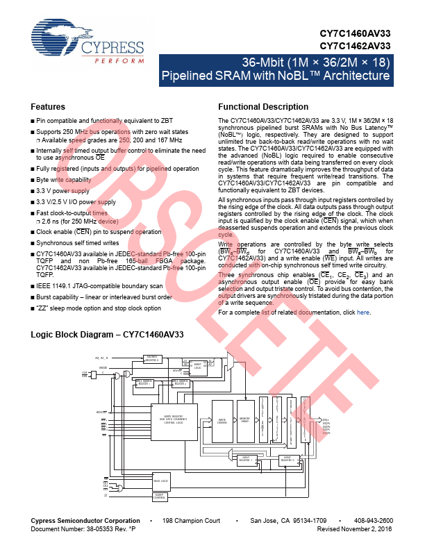
The CY7C1460AV33/CY7C1462AV33 are 3.3 V, 1M × 36/2M × 18 synchronous pipelined burst SRAMs with No Bus Latency™ (NoBL logic, respectively.
They are designed to support unlimited true back-to-back read/write operations with no wait states.
| Part number | CY7C1464AV33 |
|---|---|
| Manufacturer | Cypress (Infineon) |
| File Size | 833.98 KB |
| Description | (CY7C146xAV33) 36-Mbit Pipelined SRAM |
| Datasheet |
CY7C1464AV33 Datasheet
|
|
|
|
| Part Number | Description | Manufacturer |
|---|---|---|
| CY7C1460SV25 | 36-Mbit (1M x 36/2M x 18) Pipelined SRAM | Cypress |
| CY7C1462SV25 | 36-Mbit (1M x 36/2M x 18) Pipelined SRAM | Cypress |
| CY7C1006D | 1-Mbit (256K x 4) Static RAM | Cypress |
| CY7C1011G | 2-Mbit (128K words x 16 bit) Static RAM | Cypress |
| CY7C1041G | 4-Mbit (256K words x 16 bit) Static RAM | Cypress |
| Part Number | Description |
|---|---|
| CY7C1464AV25 | 36-Mbit (1M x 36/2M x 18/512K x 72) Pipelined SRAM |
| CY7C146 | 2K x 8 Dual-Port Static RAM |
| CY7C1460AV25 | 36-Mbit (1M x 36/2M x 18/512K x 72) Pipelined SRAM |
| CY7C1460AV33 | 36-Mbit Pipelined SRAM |
| CY7C1460BV25 | 36-Mbit (1 M x 36/2 M x 18) Pipelined SRAM |
The following content is an automatically extracted verbatim text from the original manufacturer datasheet and is provided for reference purposes only.