Datasheet4U Logo Datasheet4U.com

CY7C1419AV18 - 1.8V Synchronous Pipelined SRAM

Download the CY7C1419AV18 datasheet PDF. This datasheet also covers the CY7C1417AV18 variant, as both devices belong to the same 1.8v synchronous pipelined sram family and are provided as variant models within a single manufacturer datasheet.

Features

  • 36-Mbit density (4M x 8, 4M x 9, 2M x 18, 1M x 36).
  • 300-MHz clock for high bandwidth.
  • 4-Word burst for reducing address bus frequency.
  • Double Data Rate (DDR) interfaces (data transferred at 600 MHz) @ 300 MHz.
  • Two input clocks (K and K) for precise DDR timing.
  • SRAM uses rising edges only.
  • Two input clocks for output data (C and C) to minimize clock-skew and flight-time mismatches.
  • Echo clocks (CQ and CQ) simplify data captu.

📥 Download Datasheet

Note: The manufacturer provides a single datasheet file (CY7C1417AV18-CypressSemiconductor.pdf) that lists specifications for multiple related part numbers.

Full PDF Text Transcription

Click to expand full text
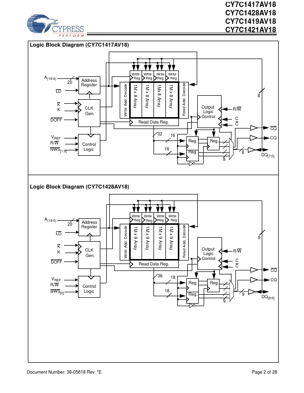
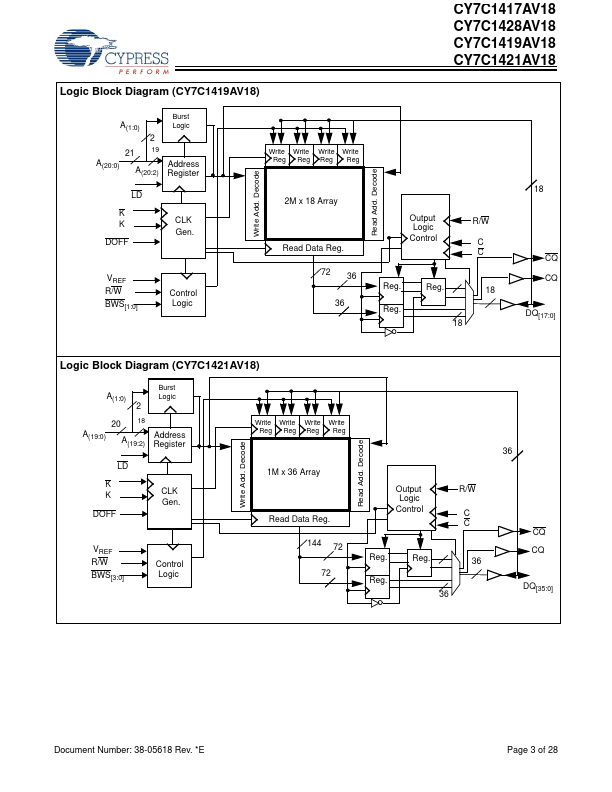
CY7C1417AV18 CY7C1428AV18 CY7C1419AV18 CY7C1421AV18 36-Mbit DDR-II SRAM 4-Word Burst Architecture Features • 36-Mbit density (4M x 8, 4M x 9, 2M x 18, 1M x 36) • 300-MHz clock for high bandwidth • 4-Word burst for reducing address bus frequency • Double Data Rate (DDR) interfaces (data transferred at 600 MHz) @ 300 MHz • Two input clocks (K and K) for precise DDR timing — SRAM uses rising edges only • Two input clocks for output data (C and C) to minimize clock-skew and flight-time mismatches • Echo clocks (CQ and CQ) simplify data capture in high-speed systems • Synchronous internally self-timed writes • 1.8V core power supply with HSTL inputs and outputs • Variable drive HSTL output buffers • Expanded HSTL output voltage (1.4V–VDD) • Available in 165-ball FBGA package (15 x 17 x 1.
Published: |