Datasheet Details
| Part number | CY7C1382BV25 |
|---|---|
| Manufacturer | Cypress (Infineon) |
| File Size | 649.04 KB |
| Description | 512K x 36 / 1 Mb x 18 Pipelined SRAM |
| Datasheet |
 CY7C1382BV25 Datasheet CY7C1382BV25 Datasheet
|
|
|
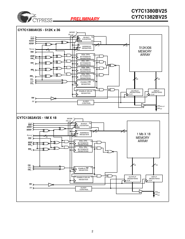
The Cypress Synchronous Burst SRAM family employs high-speed, low-power CMOS designs using advanced single-layer polysilicon, triple-layer metal technology.
Each memory cell consists of six transistors.
| Part number | CY7C1382BV25 |
|---|---|
| Manufacturer | Cypress (Infineon) |
| File Size | 649.04 KB |
| Description | 512K x 36 / 1 Mb x 18 Pipelined SRAM |
| Datasheet |
CY7C1382BV25 Datasheet
|
|
|
|
| Part Number | Description | Manufacturer |
|---|---|---|
| CY7C1382S | 18-Mbit (512 K x 36/1 M x 18) Pipelined SRAM | Cypress |
| CY7C1380S | 18-Mbit (512 K x 36/1 M x 18) Pipelined SRAM | Cypress |
| CY7C1381D | 18-Mbit (512K x 36/1M x 18) Flow-Through SRAM | Cypress |
| CY7C1383D | 18-Mbit (512K x 36/1M x 18) Flow-Through SRAM | Cypress |
| CY7C1383F | 18-Mbit (512K x 36/1M x 18) Flow-Through SRAM | Cypress |
| Part Number | Description |
|---|---|
| CY7C1382C | 18-Mb (512K x 36/1M x 18) Pipelined SRAM |
| CY7C1382CV25 | (CY7C1380CV25 / CY7C1382CV25) 512K x 36/1M x 18 Pipelined SRAM |
| CY7C1382D | 18-Mbit Pipelined SRAM |
| CY7C1382DV33 | 18-Mbit Pipelined SRAM |
| CY7C1382KV33 | 18-Mbit Pipelined SRAM |