Datasheet Details
| Part number | CY7C1145V18 |
|---|---|
| Manufacturer | Cypress (Infineon) |
| File Size | 1.18 MB |
| Description | (CY7C11xxV18) SRAM 4-Word Burst Architecture |
| Datasheet |
 CY7C1145V18 Datasheet CY7C1145V18 Datasheet
|
|
|
Download the CY7C1145V18 datasheet PDF. This datasheet also covers the CY7C1141V18 variant, as both devices belong to the same (cy7c11xxv18) sram 4-word burst architecture family and are provided as variant models within a single manufacturer datasheet.
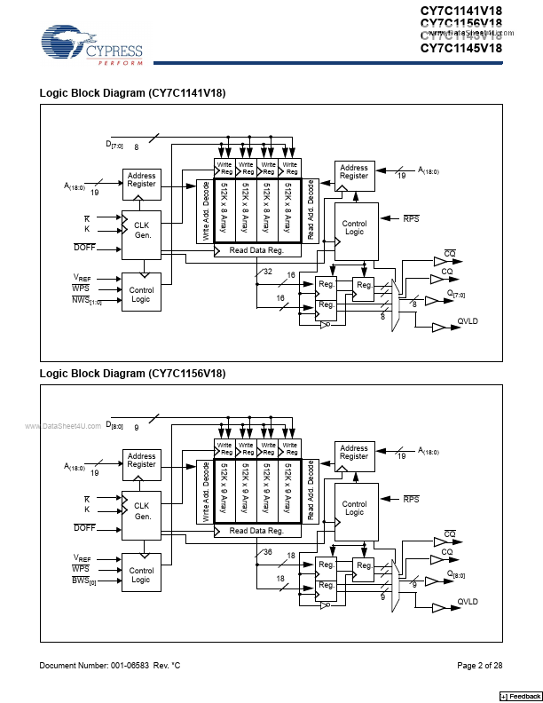
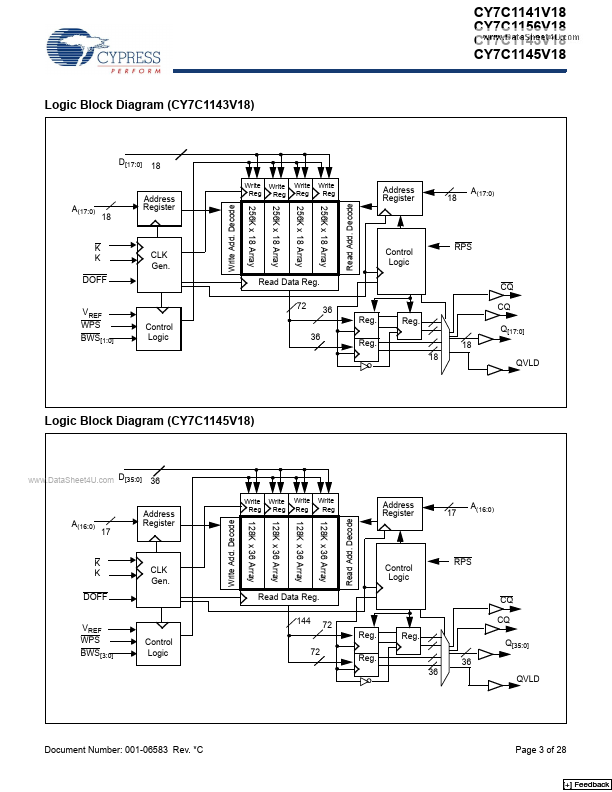
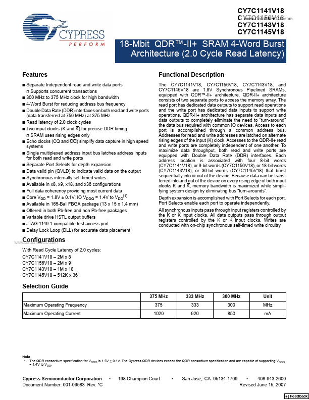
The CY7C1141V18, CY7C1156V18, CY7C1143V18, and CY7C1145V18 are 1.8V Synchronous Pipelined SRAMs, equipped with QDR™-II+ architecture.
QDR-II+ architecture consists of two separate ports to access the memory array.
| Part number | CY7C1145V18 |
|---|---|
| Manufacturer | Cypress (Infineon) |
| File Size | 1.18 MB |
| Description | (CY7C11xxV18) SRAM 4-Word Burst Architecture |
| Datasheet |
CY7C1145V18 Datasheet
|
|
|
|
| Part Number | Description | Manufacturer |
|---|---|---|
| CY7C1006D | 1-Mbit (256K x 4) Static RAM | Cypress |
| CY7C1011G | 2-Mbit (128K words x 16 bit) Static RAM | Cypress |
| CY7C1041G | 4-Mbit (256K words x 16 bit) Static RAM | Cypress |
| CY7C1041GE | 4-Mbit (256K words x 16 bit) Static RAM | Cypress |
| CY7C1041GN | 4-Mbit (256K words x 16 bit) Static RAM | Cypress |
| Part Number | Description |
|---|---|
| CY7C1145KV18 | 18-Mbit QDR II+ SRAM Four-Word Burst Architecture |
| CY7C1141V18 | (CY7C11xxV18) SRAM 4-Word Burst Architecture |
| CY7C1143KV18 | 18-Mbit QDR II+ SRAM Four-Word Burst Architecture |
| CY7C1143V18 | (CY7C11xxV18) SRAM 4-Word Burst Architecture |
| CY7C1146V18 | (CY7C11xxV18) 18-Mbit DDR-II SRAM 2-Word Burst Architecture |