Click to expand full text
07B
CY7C107B CY7C1007B
1M x 1 Static RAM
Features
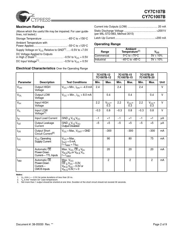
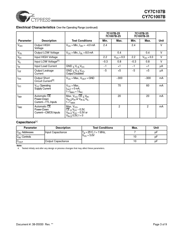
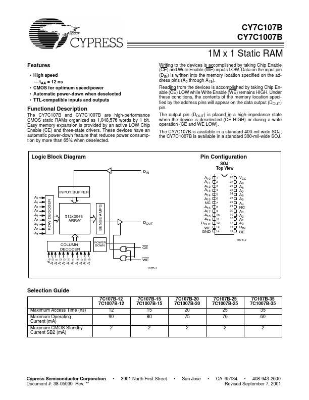
• High speed — tAA = 12 ns • CMOS for optimum speed/power • Automatic power-down when deselected • TTL-compatible inputs and outputs Writing to the devices is accomplished by taking Chip Enable (CE) and Write Enable (WE) inputs LOW. Data on the input pin (DIN) is written into the memory location specified on the address pins (A0 through A19). Reading from the devices is accomplished by taking Chip Enable (CE) LOW while Write Enable (WE) remains HIGH. Under these conditions, the contents of the memory location specified by the address pins will appear on the data output (DOUT) pin. The output pin (DOUT) is placed in a high-impedance state when the device is deselected (CE HIGH) or during a write operation (CE and WE LOW).
 CY7C107B Datasheet