Click to expand full text
CY2DL1510
1:10 Differential LVDS Fanout Buffer
1:10 Differential LVDS Fanout Buffer
Features
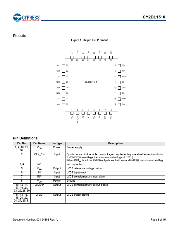
■ Low-voltage differential signal (LVDS) input with on-chip 100 input termination resistor
■ Ten differential LVDS outputs ■ 40 ps maximum output-to-output skew ■ 600 ps maximum propagation delay ■ 0.11 ps maximum additive RMS phase jitter at 156.25 MHz
(12 kHz to 20 MHz offset) ■ Up to 1.5 GHz operation ■ Synchronous clock enable function ■ 32-pin thin quad flat pack (TQFP) package ■ 2.5 V or 3.3 V operating voltage [1] ■ Commercial and industrial operating temperature range
Functional Description
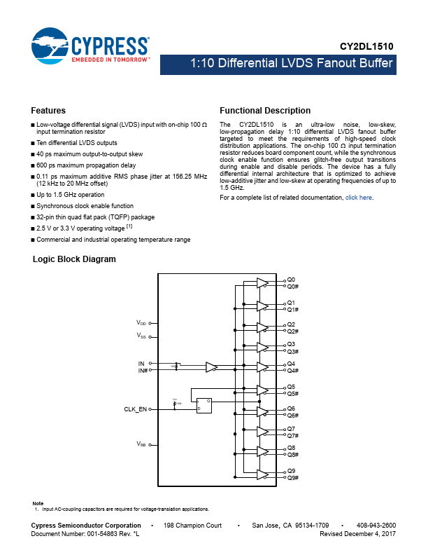
The CY2DL1510 is an ultra-low noise, low-skew, low-propagation delay 1:10 differential LVDS fanout buffer targeted to meet the requirements of high-speed clock distribution applications.
 CY2DL1510 Datasheet