The following content is an automatically extracted verbatim text
from the original manufacturer datasheet and is provided for reference purposes only.
View original datasheet text
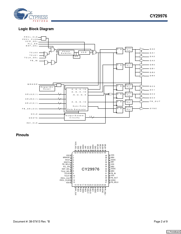
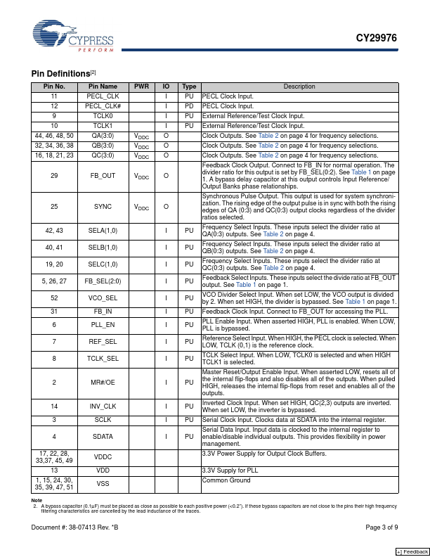
CY29976
3.3V, 125-MHz, Multi-Output Zero Delay Buffer
Features
■ ■ ■ ■ ■ ■
Output frequency up to 125 MHz Supports PowerPC , and Pentium processors 12 clock outputs: frequency configurable Configurable Output Disable Two reference clock inputs for dynamic toggling Oscillator or PECL reference input
® ®
■ ■ ■ ■ ■ ■
Spread spectrum compatible Glitch-free output clocks transitioning 3.3V power supply Pin compatible with SC973X Industrial temperature range: –40°C to +85°C 52-Pin TQFP package
Table 1. Frequency Table[1] VC0_SEL 0 0 0 0 0 0 0 0 1 1 1 1 1 1 1 1 FB_SEL2 0 0 0 0 1 1 1 1 0 0 0 0 1 1 1 1 FB_SEL1 0 0 1 1 0 0 1 1 0 0 1 1 0 0 1 1 FB_SEL0 0 1 0 1 0 1 0 1 0 1 0 1 0 1 0 1 FVCO 8x 12x 16x 20x 8x 12x 16x 20x 4x 6x 8x 10x 4x 6x 8x 10x
Note 1.
 CY29976 Datasheet