Click to expand full text
CY28517
PCI Express Clock Generator
Features
■ ■ ■ ■ ■ ■ ■ ■ ■ ■ ■
Selectable, Triangle, and Lexmark profiles SMbus support with readback capabilities 3.3V power supply Packages are Pb free and ROHS compliant 28-pin TSSOP packages 100M x4 25M x2 27M x1 48M x1
Four 100 MHz differential clocks 48 MHz clock Two 25 MHz clocks 27 MHz Reference Clock OE control per clock output Selectable drive strength per output
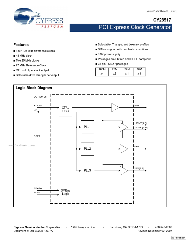
Logic Block Diagram
OE_100_25
X1/CLK X2
XTAL OSC
27M
100MT[A:D]
PLL1
RSET
100MC[A:D]
www.DataSheet4U.com
PLL2
48M
PLL3
25M[A:B]
SDATA SCLK
SMBus Logic
Cypress Semiconductor Corporation Document #: 001-42225 Rev. *A
•
198 Champion Court
•
San Jose, CA 95134-1709 • 408-943-2600 Revised November 02, 2007
[+] Feedback
CY28517
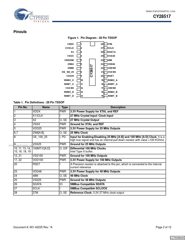
Pinouts
Figure 1.
 CY28517 Datasheet