Datasheet Details
| Part number | CY2509 |
|---|---|
| Manufacturer | Cypress (now Infineon) |
| File Size | 276.00 KB |
| Description | (CY2509 / CY2510) Ten/Eleven Output Zero Delay Buffer |
| Datasheet |
 CY2509 Datasheet CY2509 Datasheet
|
|
|
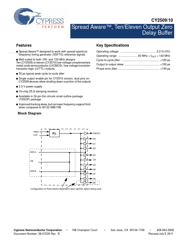
This page provides the datasheet information for the CY2509, a member of the CY2510 (CY2509 / CY2510) Ten/Eleven Output Zero Delay Buffer family.
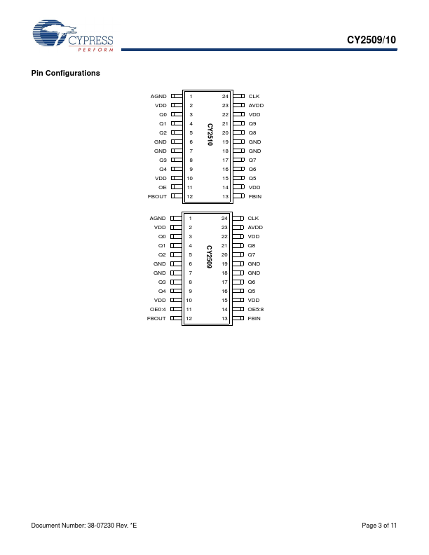
Reference input: Output signals Q0:9 will be synchronized to this signal.
Feedback input: This input must be fed by one of the outputs (typically FBOUT) to ensure proper functionality.
| Part number | CY2509 |
|---|---|
| Manufacturer | Cypress (now Infineon) |
| File Size | 276.00 KB |
| Description | (CY2509 / CY2510) Ten/Eleven Output Zero Delay Buffer |
| Datasheet |
CY2509 Datasheet
|
|
|
|