Datasheet4U Logo Datasheet4U.com

CEG9926 - Dual N-Channel Enhancement Mode Field Effect Transistor

Download the CEG9926 datasheet PDF. This datasheet also covers the CEG9926_Chino variant, as both devices belong to the same dual n-channel enhancement mode field effect transistor family and are provided as variant models within a single manufacturer datasheet.

Key Features

  • 20V , 4.5A , RDS(ON)=30mΩ @VGS=4.5V. RDS(ON)=40m Ω @VGS=2.5V. Super high dense cell design for extremely low RDS(ON). High power and current handing capability. TSSOP-8 for Surface Mount Package. G2 S2 S2 D2 D1 1 S1 2 S1 3 G1 4 8 D2 7 S2 6 S2 5 G2 ȀȀȀ Parameter Drain-Source Voltage Gate-Source Voltage Drain Current-Continuous a b -Pulsed Drain-Source Diode Forward Current a Maximum Power Dissipation a Operating Junction and Storage Temperature Range G1 S1 S1 D1 9 TSSOP-8.

📥 Download Datasheet

Note: The manufacturer provides a single datasheet file (CEG9926_Chino-ExcelTechnology.pdf) that lists specifications for multiple related part numbers.

Datasheet Details

Part number CEG9926
Manufacturer Chino-Excel Technology
File Size 56.15 KB
Description Dual N-Channel Enhancement Mode Field Effect Transistor
Datasheet download datasheet CEG9926 Datasheet

Full PDF Text Transcription (Reference)

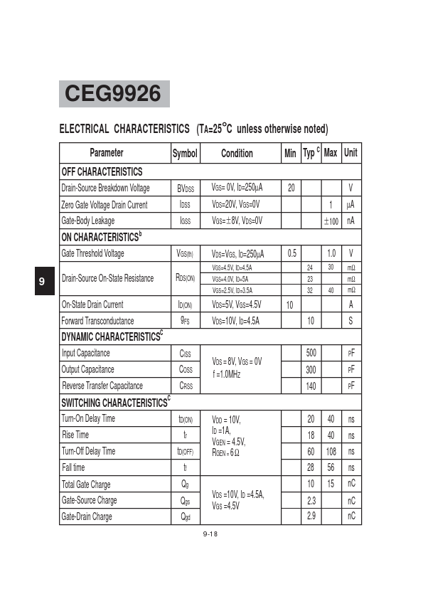
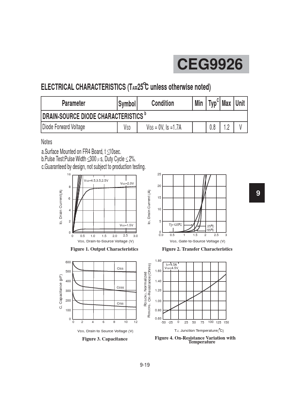
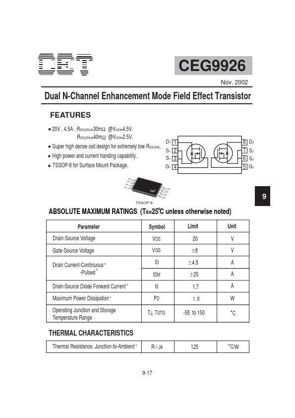
The following content is an automatically extracted verbatim text from the original manufacturer datasheet and is provided for reference purposes only.

View original datasheet text
CEG9926 Nov. 2002 Dual N-Channel Enhancement Mode Field Effect Transistor FEATURES 20V , 4.5A , RDS(ON)=30mΩ @VGS=4.5V. RDS(ON)=40m Ω @VGS=2.5V. Super high dense cell design for extremely low RDS(ON). High power and current handing capability. TSSOP-8 for Surface Mount Package. G2 S2 S2 D2 D1 1 S1 2 S1 3 G1 4 8 D2 7 S2 6 S2 5 G2 ȀȀȀ Parameter Drain-Source Voltage Gate-Source Voltage Drain Current-Continuous a b -Pulsed Drain-Source Diode Forward Current a Maximum Power Dissipation a Operating Junction and Storage Temperature Range G1 S1 S1 D1 9 TSSOP-8 ABSOLUTE MAXIMUM RATINGS (TA=25 C unless otherwise noted) Symbol VDS VGS ID IDM IS PD TJ, TSTG Limit 20 Ć8 Ć4.5 Unit V V A A A W C Ć25 1.