|
CP600
|
SINGLE-PHASE SILICON BRIDGE-P.C. MTG 3A / HEAT-SINK MTG 6A(VOLTAGE 50 to 1000 Volts CURRENT - P.C. MTG 3A / HEAT-SINK MTG 6A) |
Pan Jit International Inc. |
|
CP600
|
SINGLE-PHASE SILICON BRIDGE-P.C. MTG 3A/ HEAR-SINK MTG 6A |
TRSYS |
|
CP601
|
SINGLE-PHASE SILICON BRIDGE-P.C. MTG 3A / HEAT-SINK MTG 6A(VOLTAGE 50 to 1000 Volts CURRENT - P.C. MTG 3A / HEAT-SINK MTG 6A) |
Pan Jit International Inc. |
|
CP601
|
SINGLE-PHASE SILICON BRIDGE-P.C. MTG 3A/ HEAR-SINK MTG 6A |
TRSYS |
|
CP6010
|
SINGLE-PHASE SILICON BRIDGE-P.C. MTG 3A / HEAT-SINK MTG 6A(VOLTAGE 50 to 1000 Volts CURRENT - P.C. MTG 3A / HEAT-SINK MTG 6A) |
Pan Jit International Inc. |
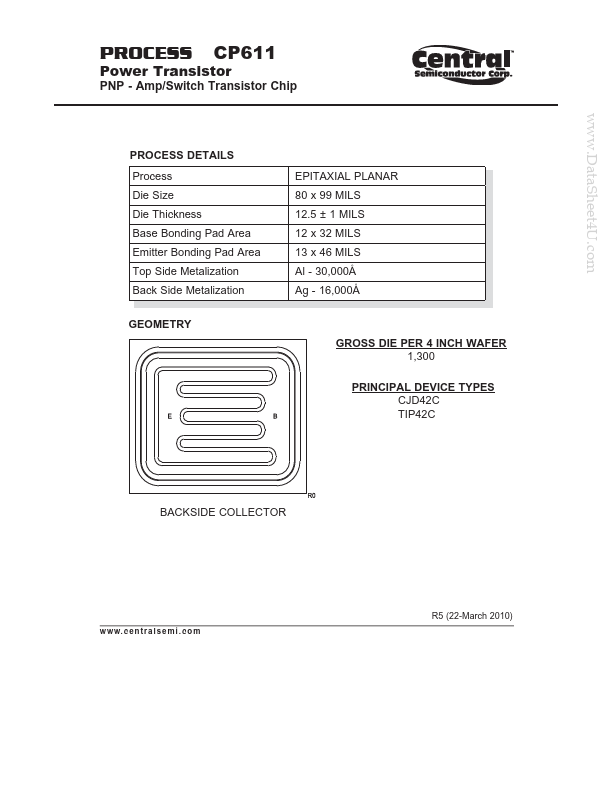
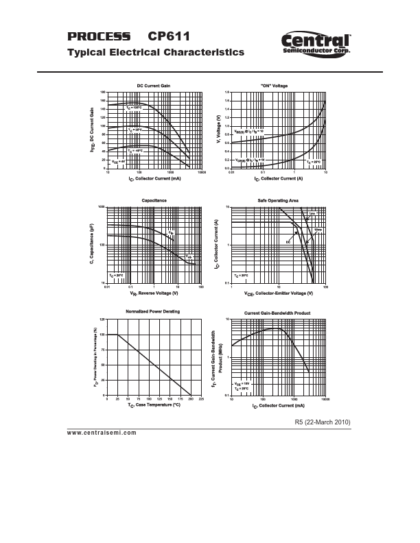
 CP611 Datasheet