Click to expand full text
CEH2609
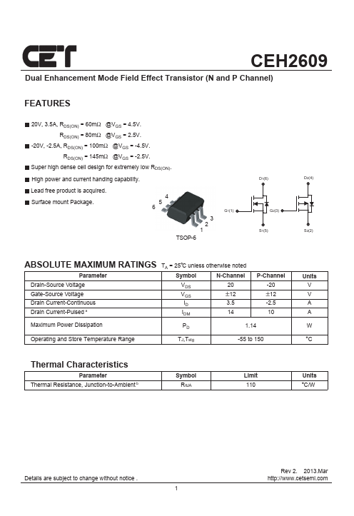
Dual Enhancement Mode Field Effect Transistor (N and P Channel)
FEATURES
20V, 3.5A, RDS(ON) = 60mΩ @VGS = 4.5V. RDS(ON) = 80mΩ @VGS = 2.5V.
-20V, -2.5A, RDS(ON) = 100mΩ @VGS = -4.5V. RDS(ON) = 145mΩ @VGS = -2.5V.
Super high dense cell design for extremely low RDS(ON).
High power and current handing capability.
Lead free product is acquired. Surface mount Package.
4 5 6
3 2 1 TSOP-6
G1(1)
D1(6)
G2(3) S1(5)
D2(4) S2(2)
ABSOLUTE MAXIMUM RATINGS TA = 25 C unless otherwise noted
Parameter
Symbol
N-Channel
Drain-Source Voltage Gate-Source Voltage Drain Current-Continuous Drain Current-Pulsed a
VDS 20
VGS ±12
ID 3.5 IDM 14
P-Channel -20
±12
-2.5 10
Maximum Power Dissipation
PD 1.
 CEH2609 Datasheet