Datasheet4U Logo Datasheet4U.com

B3965D - N- and P-Channel 40-V (D-S) MOSFET

Description

The B3965D is the N- and P-Channel logic enhancement mode power field effect transistors are produced using high cell density, DMOS trench technology.

This high density process is especially tailored to minimize on-state resistance.

Features

  • 40V/5.2A, RDS(ON)=40mΩ@VGS=10V (N-Ch) 40V/4.9A, RDS(ON)=45mΩ@VGS=4.5V (N-Ch) -40V/-4.5A, RDS(ON)=54mΩ@VGS=-10V (P-Ch) -40V/-3.9A, RDS(ON)=72mΩ@VGS=-4.5V (P-Ch) Super High Density Cell Design For Extremely Low RDS(ON) Exceptional On-Resistance and Maximum DC Current Capability TO-252 Package.

📥 Download Datasheet

Datasheet Details

Part number B3965D
Manufacturer BiTEK
File Size 59.65 KB
Description N- and P-Channel 40-V (D-S) MOSFET
Datasheet download datasheet B3965D Datasheet

Full PDF Text Transcription

Click to expand full text
B3965D N- and P-Channel 40-V (D-S) MOSFET General Description The B3965D is the N- and P-Channel logic enhancement mode power field effect transistors are produced using high cell density, DMOS trench technology. This high density process is especially tailored to minimize on-state resistance. These devices are particularly suited for low voltage application such as cellular phone and notebook computer power management and other battery powered circuits with high-side switching, and low in-line power loss are needed in a very small outline surface mount package.
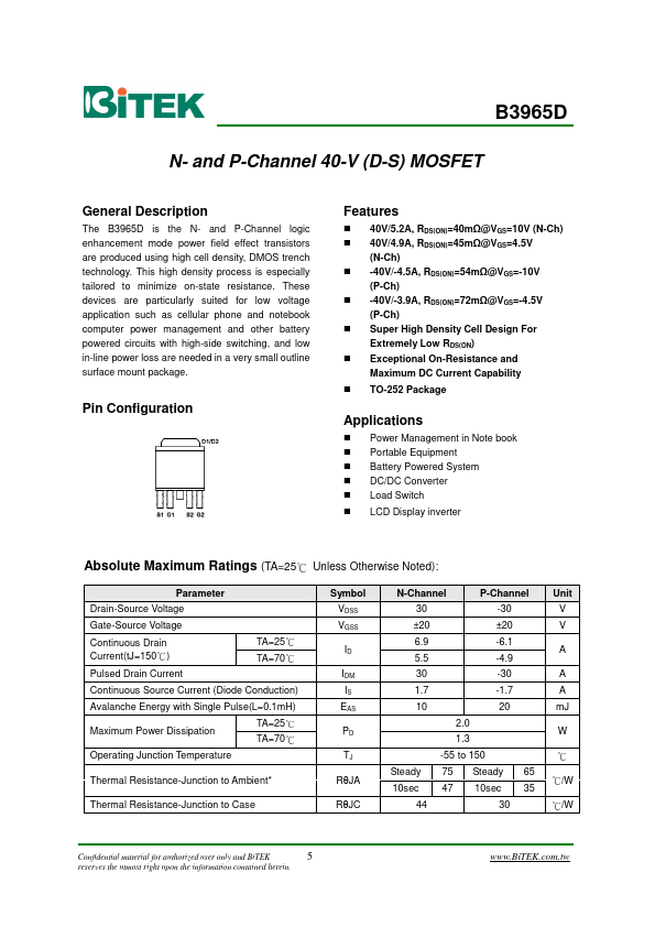
 Pin Configuration Features 40V/5.2A, RDS(ON)=40mΩ@VGS=10V (N-Ch) 40V/4.9A, RDS(ON)=45mΩ@VGS=4.5V (N-Ch) -40V/-4.5A, RDS(ON)=54mΩ@VGS=-10V (P-Ch) -40V/-3.9A, RDS(ON)=72mΩ@VGS=-4.
Published: |