Datasheet Details
| Part number | BF90315SNS |
|---|---|
| Manufacturer | BYD |
| File Size | 175.64 KB |
| Description | N-Channel MOSFET |
| Datasheet |
 BF90315SNS Datasheet BF90315SNS Datasheet
|
|
|
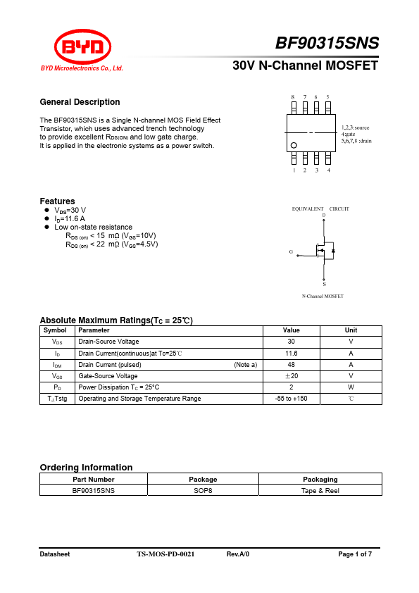
The BF90315SNS is a Single N-channel MOS Field Effect Transistor, which uses advanced trench technology to provide excellent RDS(ON) and low gate charge.
It is applied in the electronic systems as a power switch.
| Part number | BF90315SNS |
|---|---|
| Manufacturer | BYD |
| File Size | 175.64 KB |
| Description | N-Channel MOSFET |
| Datasheet |
BF90315SNS Datasheet
|
|
|
|