Datasheet Details
| Part number | BF9028DND-GE |
|---|---|
| Manufacturer | BYD |
| File Size | 213.31 KB |
| Description | N-Channel MOSFET |
| Datasheet |
 BF9028DND-GE Datasheet BF9028DND-GE Datasheet
|
|
|
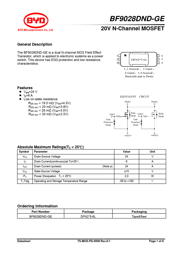
The BF9028DND-GE is a dual N-channel MOS Field Effect Transistor, which is applied to electronic systems as a power switch.
This device has ESD-protection and low resistance characteristics.
| Part number | BF9028DND-GE |
|---|---|
| Manufacturer | BYD |
| File Size | 213.31 KB |
| Description | N-Channel MOSFET |
| Datasheet |
BF9028DND-GE Datasheet
|
|
|
|