Datasheet Details
| Part number | BF9024SPD-M |
|---|---|
| Manufacturer | BYD |
| File Size | 364.90 KB |
| Description | P-Channel MOSFET and Schottky Diode |
| Datasheet |
 BF9024SPD-M Datasheet BF9024SPD-M Datasheet
|
|
|
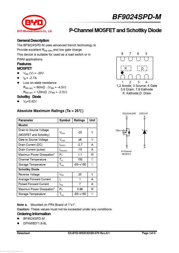
The BF9024SPD-M uses advanced trench technology to Provide excellent RDS (ON) and low gate charge.
This device is suitable for used as a load switch or in PWM applications.
| Part number | BF9024SPD-M |
|---|---|
| Manufacturer | BYD |
| File Size | 364.90 KB |
| Description | P-Channel MOSFET and Schottky Diode |
| Datasheet |
BF9024SPD-M Datasheet
|
|
|
|