The following content is an automatically extracted verbatim text
from the original manufacturer datasheet and is provided for reference purposes only.
View original datasheet text
Apm JFET
2SK117
Low Noise Amplifier Applications Silicon N Channel Junction Type
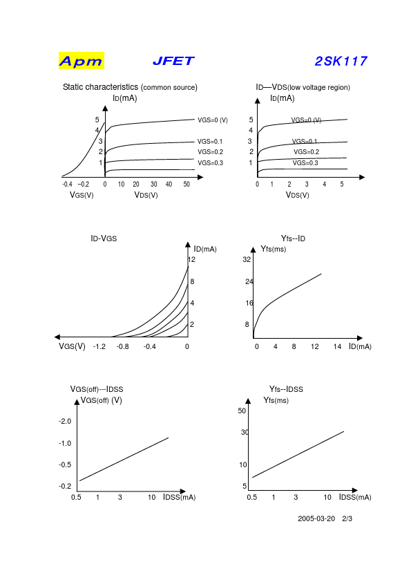
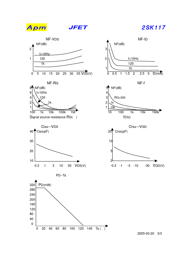
*High Yfs=15ms(typ)(VDS=10V,VGS=0) *High VGDS=--30V *Low noise:NF=1.0dB(typ)
(VDS=10V,ID=0.5mA,f=1kHz,RG=1k ) *High input impedance:IGSS=-1nA,VGS=-30V)
Absolute Maximum rating at Ta=25
SYMBOL
VGDS IG
Tstg Tj
PD
PARAMETER Gate-Drain voltage
Gate current storage temprature operating junction temperature Drain power dissipation
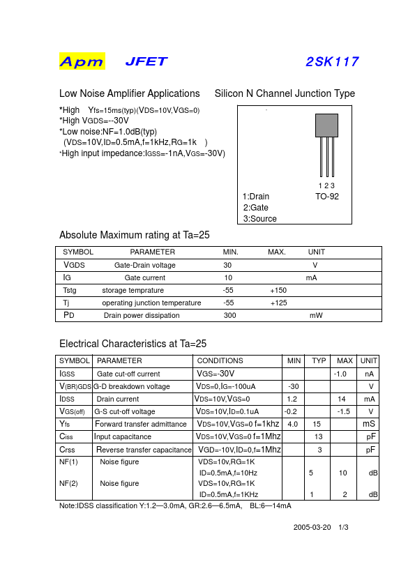
1:Drain 2:Gate 3:Source
MIN. 30 10 -55 -55 300
MAX.
+150 +125
123
TO-92
UNIT V
mA
mW
Electrical Characteristics at Ta=25
SYMBOL PARAMETER
CONDITIONS
MIN
IGSS
Gate cut-off current
VGS=-30V
V(BR)GDS G-D breakdown voltage
VDS=0,IG=-100uA
-30
IDSS
Drain current
VDS=10V,VGS=0
1.2
VGS(off) G-S cut-off voltage
VDS=10V,ID=0.1uA
-0.
 2SK117 Datasheet