Description
Specifications 4
Timing Characteristics10 Absolute Maximum Ratings 13
Thermal Resistance 13 ESD Caution13 Pin Configuration and Function Descriptions 14 Typical Performance Characteristics 17 Terminology 26 RMS Noise and Resolution 27 Full Power Mode 27 Mid Power Mode 30 Low Power Mode33 Getting Started 36 Overview 36 Power Supplies 37 Digital Communication 37 Configuration Overview 39 ADC Circuit Information46 Analog Input Channel46 Programmable Gain Amplifier (PGA) 47 Reference47 Bipolar/Uni
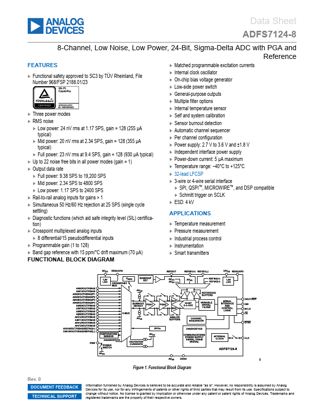
Features
- Functional safety approved to SC3 by TÜV Rheinland, File Number 968/FSP 2188.01/23.
- Three power modes.
- RMS noise.
- Low power: 24 nV rms at 1.17 SPS, gain = 128 (255 µA typical).
- Mid power: 20 nV rms at 2.34 SPS, gain = 128 (355 µA typical).
- Full power: 23 nV rms at 9.4 SPS, gain = 128 (930 µA typical).
- Up to 22 noise free bits in all power modes (gain = 1).
- Output data rate.
- Full power: 9.38 SPS to 19,200 SPS.
- Mid power: 2.34 SPS to 4800 SPS.
 ADFS7124-8 Datasheet