Datasheet Details
| Part number | AOB66918L |
|---|---|
| Manufacturer | Alpha & Omega Semiconductors |
| File Size | 377.53 KB |
| Description | 100V N-Channel MOSFET |
| Datasheet |
 AOB66918L Datasheet AOB66918L Datasheet
|
|
|
| Part number | AOB66918L |
|---|---|
| Manufacturer | Alpha & Omega Semiconductors |
| File Size | 377.53 KB |
| Description | 100V N-Channel MOSFET |
| Datasheet |
AOB66918L Datasheet
|
|
|
|
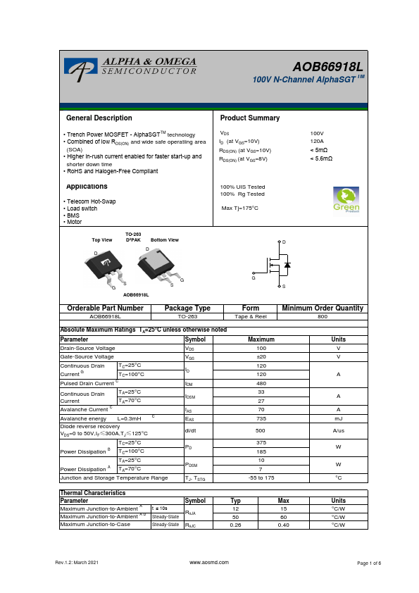
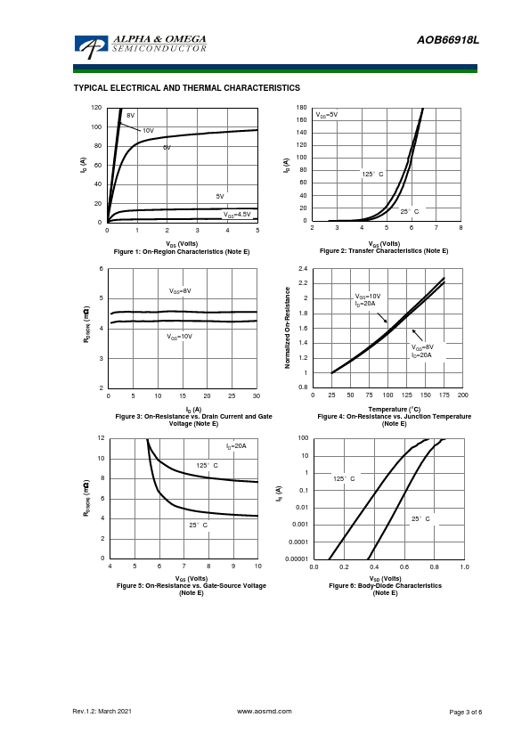
• Trench Power MOSFET - AlphaSGTTM technology • Combined of low RDS(ON) and wide safe operatiing area (SOA) • Higher in-rush current enabled for faster start-up and shorter down time • RoHS and Halogen-Free Compliant Applications • Telecom Hot-Swap • Load switch • BMS • Motor Top View D TO-263 D2PAK Bottom View D Product Summary VDS ID (at VGS=10V) RDS(ON) (at VGS=10V) RDS(ON) (at VGS=8V) 100% UIS Tested 100% Rg Tested Max Tj=175°C D 100V 120A < 5mΩ < 5.6mΩ S G AOB66918L G S G S Orderable Part Number AOB66918L Package Type TO-263 Form Tape & Reel Minimum Order Quantity 800 Absolute Maximum Ratings TA=25°C unless otherwise noted Parameter Symbol Drain-Source Voltage VDS Gate-Source Voltage VGS Continuous Drain Current G TC=25°C TC=100°C ID Pulsed Drain Current C IDM Continuous Drain Current TA=25°C TA=70°C IDSM Avalanche Current C IAS Avalanche energy L=0.3mH C EAS Diode reverse recovery VDS=0 to 50V,IF≤300A,TJ≤125°C di/dt TC=25°C Power Dissipation B TC=100°C PD TA=25°C Power Dissipation A TA=70°C PDSM Junction and Storage Temperature Range TJ, TSTG Maximum 100 ±20 120 120 480 33 27 70 735 500 375 185 10 7 -55 to 175 Units V V A A A mJ A/us W W °C Thermal Characteristics Parameter Maximum Junction-to-Ambient A Maximum Junction-to-Ambient A D Maximum Junction-to-Case t ≤ 10s Steady-State Steady-State Symbol RqJA RqJC Typ 12 50 0.26 Max 15 60 0.40 Units °C/W °C/W °C/W Rev.1.2: March 2021 www.aosmd.com Page 1 of 6 AOB66918L Electrical Characteristics (TJ=25°C unless otherwise noted) Symbol Parameter Conditions Min STATIC PARAMETERS BVDSS Drain-Source Breakdown Voltage ID=250mA, VGS=0V 100 IDSS Zero Gate Voltage Drain Current VDS=100V, VGS=0V TJ=55°C IGSS Gate-Body leakage current VDS=0V, VGS=±20V VGS(th) Gate Threshold Voltage VDS=VGS, ID=250mA 2.7 VGS=10V, ID=20A RDS(ON) Static Drain-Source On-Resistance TJ=125°C VGS=8V, ID=20A gFS Fo
AOB66918L 100V N-Channel AlphaSGT TM General.
| Part Number | Description |
|---|---|
| AOB66914L | 100V N-Channel MOSFET |
| AOB66919L | 100V N-Channel MOSFET |
| AOB66935L | 100V N-Channel MOSFET |
| AOB66518L | 150V N-Channel MOSFET |
| AOB66613L | 60V N-Channel MOSFET |
| AOB66616L | N-Channel MOSFET |
| AOB66620L | 60V N-Channel MOSFET |
| AOB600A60L | 600V N-Channel Power Transistor |
| AOB600A70FL | N-Channel Power Transistor |
| AOB600A70L | 700V N-Channel Power Transistor |