Datasheet Details
| Part number | AO4817 |
|---|---|
| Manufacturer | Alpha & Omega Semiconductors |
| File Size | 132.84 KB |
| Description | Dual P-Channel MOSFET |
| Datasheet |
 AO4817 Datasheet AO4817 Datasheet
|
|
|
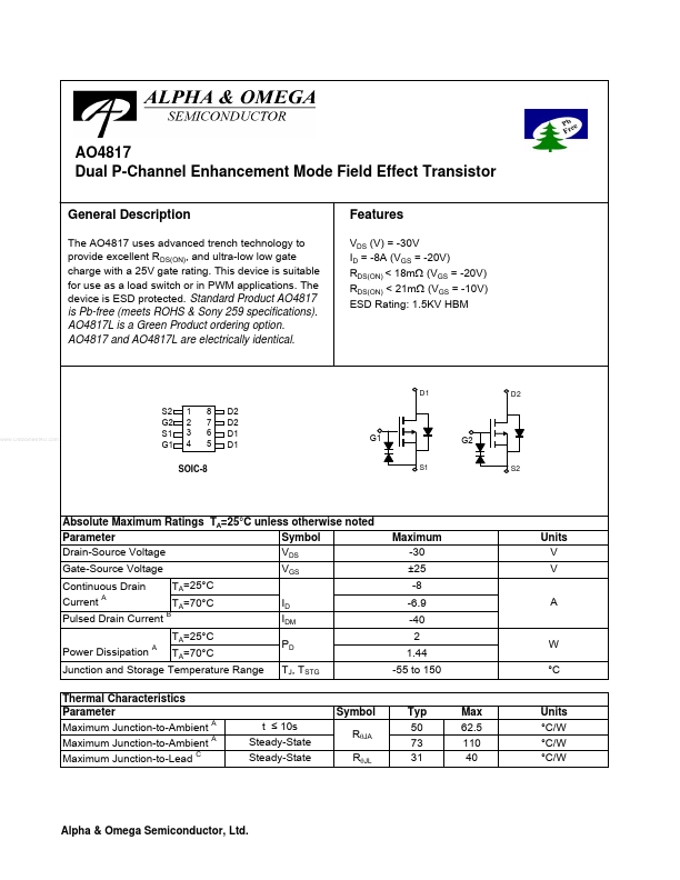
The AO4817 uses advanced trench technology to provide excellent RDS(ON), and ultra-low low gate charge with a 25V gate rating.
This device is suitable for use as a load switch or in PWM applications.
The device is ESD protected.
| Part number | AO4817 |
|---|---|
| Manufacturer | Alpha & Omega Semiconductors |
| File Size | 132.84 KB |
| Description | Dual P-Channel MOSFET |
| Datasheet |
AO4817 Datasheet
|
|
|
|
| Part Number | Description | Manufacturer |
|---|---|---|
| AO4817 | Dual P-Channel MOSFET | Kexin |
| AO4817-HF | Dual P-Channel MOSFET | Kexin |
| AO4811 | Dual P-Channel MOSFET | FreesCale |
| AO4812 | Dual N-Channel MOSFET | Kexin |
| AO4812 | Dual N-Channel 30V MOSFET | VBsemi |
| Part Number | Description |
|---|---|
| AO4812 | 30V Dual N-Channel MOSFET |
| AO4812A | Dual N-Channel MOSFET |
| AO4813 | 30V Dual P-Channel MOSFET |
| AO4815 | Dual P-Channel MOSFET |
| AO4816 | Dual N-Channel MOSFET |
The following content is an automatically extracted verbatim text from the original manufacturer datasheet and is provided for reference purposes only.