AS7C251MNTF18A
Features
- -
- -
- -
- - Organization: 1,048,576 words × 18 bits NTD™ architecture for efficient bus operation Fast clock to data access: 7.5/8.5/10 ns Fast OE access time: 3.5/4.0 ns Fully synchronous operation Flow-through mode Asynchronous output enable control Available in 100-pin TQFP package
- -
- -
- -
- Individual byte write and global write Clock enable for operation hold Multiple chip enables for easy expansion 2.5V core power supply Self-timed write cycles Interleaved or linear burst modes Snooze mode for standby operation
..
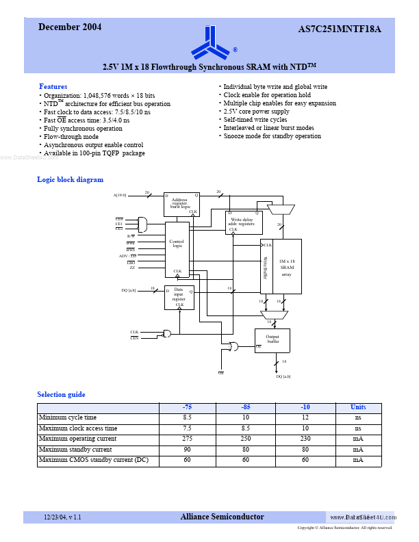
Logic block diagram
A[19:0] 20 D
Address register burst logic
CLK CE0 CE1 CE2 R/W BWa BWb ADV / LD LBO ZZ
Q 20
Write delay addr. registers
Control logic
Write Buffer
1M x 18 SRAM array
DQ [a,b]
Data Q input register
18 18 18
18 CLK CEN OE
Output buffer
18 OE
DQ [a,b]
Selection guide
-75 Minimum cycle time Maximum clock access time Maximum operating current Maximum standby current Maximum CMOS standby...