Datasheet4U Logo Datasheet4U.com

OR4E6 - Field-Programmable Gate Arrays

Download the OR4E6 datasheet PDF (OR4 included). The manufacturer datasheet provides complete specifications, pinout details, electrical characteristics, and typical applications for field-programmable gate arrays.

Description

6 Architecture Overview 6 Programmable Logic Cells 7 Programmable Function Unit 8 Look-Up Table Operating Modes 11 Supplemental Logic and Interconnect Cell 21 PLC Latches/Flip-Flops 25 Embedded Block RAM 27 EBR

Features

  • s High-performance platform design.
  • 0.13 µm seven-level metal technology.
  • Internal performance of >250 MHz (four logic levels).
  • I/O performance of >416 MHz for all user I/Os.
  • Over 1.5 million usable system gates.
  • Meets multiple I/O interface standards.
  • 1.5 V operation (30% less power than 1.8 V operation) translates to greater performance.
  • Embedded block RAM (EBR) for onboard storage and buffer needs.
  • Built-in syste.

📥 Download Datasheet

Note: The manufacturer provides a single datasheet file (OR4-E10.pdf) that lists specifications for multiple related part numbers.

Datasheet Details

Part number OR4E6
Manufacturer Agere Systems
File Size 3.06 MB
Description Field-Programmable Gate Arrays
Datasheet download datasheet OR4E6 Datasheet
Other Datasheets by Agere Systems

Full PDF Text Transcription

Click to expand full text
Preliminary Data Sheet December 2000 ORCA® Series 4 Field-Programmable Gate Arrays Programmable Features s 
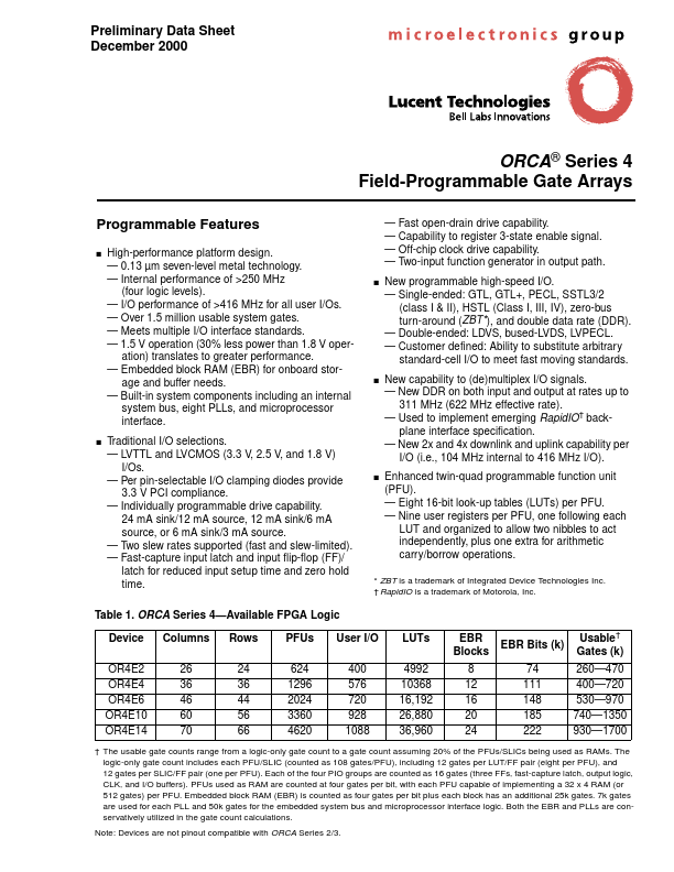
High-performance platform design. — 0.13 µm seven-level metal technology. — Internal performance of >250 MHz (four logic levels). — I/O performance of >416 MHz for all user I/Os. — Over 1.5 million usable system gates. — Meets multiple I/O interface standards. — 1.5 V operation (30% less power than 1.8 V operation) translates to greater performance. — Embedded block RAM (EBR) for onboard storage and buffer needs. — Built-in system components including an internal system bus, eight PLLs, and microprocessor interface. Traditional I/O selections. — LVTTL and LVCMOS (3.3 V, 2.5 V, and 1.8 V) I/Os. — Per pin-selectable I/O clamping diodes provide 3.3 V PCI compliance.
Published: |