ATMLH730 Datasheet Text
AT93C46D
3-wire Serial EEPROM
1K (128 x 8 or 64 x 16)
DATASHEET
Features
- Low-voltage Operation ̶ VCC = 1.8V to 5.5V
- User-selectable Internal Organization ̶ 1K: 128 x 8 or 64 x 16
- 3-wire Serial Interface
- 2MHz Clock Rate (5V)
- Self-timed Write Cycle (5ms Max)
- High Reliability
̶ Endurance: 1,000,000 Write Cycles ̶ Data Retention: 100 Years
- 8-lead JEDEC SOIC, 8-lead TSSOP, 8-pad UDFN, 8-lead PDIP, and 8-ball VFBGA Packages
Description
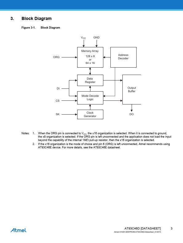
The Atmel® AT93C46D provides 1,024 bits of Serial Electrically Erasable Programmable Read-Only Memory (EEPROM) organized as 64 words of 16 bits each (when the ORG pin is connected to VCC) and 128 words of 8 bits each (when the ORG pin is tied to ground). The device is optimized for use in many industrial and mercial applications where low-power and low-voltage operations are essential. The AT93C46D is available in space-saving 8-lead JEDEC SOIC, 8-lead TSSOP, 8-pad UDFN, 8-lead PDIP, and 8-ball VFBGA packages. The AT93C46D is enabled through the Chip Select pin (CS) and accessed via a 3-wire serial interface consisting of Data Input (DI), Data Output (DO), and Shift Clock (SK). Upon receiving a Read instruction at DI, the address is decoded, and the data is clocked out serially on the DO pin. The write cycle is pletely self-timed, and no separate erase cycle is required before Write. The write cycle is only enabled when the part is in the Erase/Write Enable state. When CS is brought high following the initiation of a write cycle, the DO pin outputs the Ready/Busy status of the part. The AT93C46D operates from 1.8V to 5.5V.
Atmel-5193H-SEEPROM-AT93C46D-Datasheet_012015
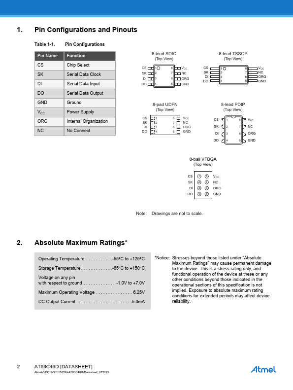
1. Pin Configurations and Pinouts
Table 1-1. Pin Configurations
Pin Name CS SK DI DO GND VCC ORG NC
Function Chip Select Serial Data Clock Serial Data...