93C46 Datasheet Text
Features
- Low-voltage and Standard-voltage Operation
- 2.7 (VCC = 2.7V to 5.5V)
- 1.8 (VCC = 1.8V to 5.5V)
- User-selectable Internal Organization
- 1K: 128 x 8 or 64 x 16
- 2K: 256 x 8 or 128 x 16
- 4K: 512 x 8 or 256 x 16
- Three-wire Serial Interface
- 2 MHz Clock Rate (5V)
- Self-timed Write Cycle (10 ms max)
- High Reliability
- Endurance: 1 Million Write Cycles
- Data Retention: 100 Years
- Automotive Grade, Extended Temperature and Lead-Free/Halogen-Free Devices Available
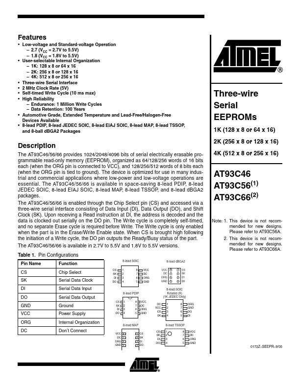
- 8-lead PDIP, 8-lead JEDEC SOIC, 8-lead EIAJ SOIC, 8-lead MAP, 8-lead TSSOP, and 8-ball dBGA2 Packages
Description
The AT93C46/56/66 provides 1024/2048/4096 bits of serial electrically erasable programmable read-only memory (EEPROM), organized as 64/128/256 words of 16 bits each (when the ORG pin is connected to VCC), and 128/256/512 words of 8 bits each (when the ORG pin is tied to ground). The device is optimized for use in many industrial and mercial applications where low-power and low-voltage operations are essential. The AT93C46/56/66 is available in space-saving 8-lead PDIP, 8-lead JEDEC SOIC, 8-lead EIAJ SOIC, 8-lead MAP, 8-lead TSSOP, and 8-lead dBGA2 packages.
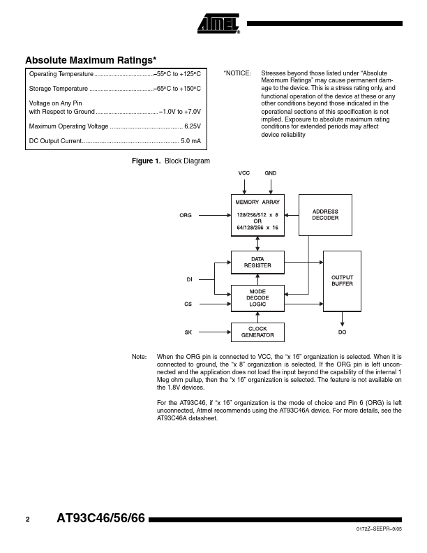
The AT93C46/56/66 is enabled through the Chip Select pin (CS) and accessed via a three-wire serial interface consisting of Data Input (DI), Data Output (DO), and Shift Clock (SK). Upon receiving a Read instruction at DI, the address is decoded and the data is clocked out serially on the DO pin. The Write cycle is pletely self-timed, and no separate Erase cycle is required before Write. The Write cycle is only enabled when the part is in the Erase/Write Enable state. When CS is brought high following the initiation of a Write cycle, the DO pin outputs the Ready/Busy status of the part.
The AT93C46/56/66 is available in...