Datasheet4U Logo Datasheet4U.com

S4850 - Dual OC-48 SONET/SDH CRU

Description

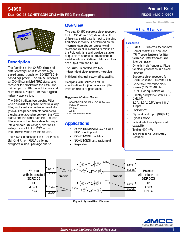
The function of the S4850 clock and data recovery unit is to derive high speed timing signals for SONET/SDHbased equipment.

The S4850 receives an OC-48 scrambled NRZ signal and recovers the clock from the data.

The chip outputs a differential bit clock and retimed data.

Features

  • es.
  • CMOS 0.13 micron technology Complies with Bellcore and ITU-T specifications for jitter tolerance, jitter transfer, and jitter generation On-chip high-frequency PLLs for clock generation and clock recovery Supports clock recovery for 2.488 Gbps (OC-48) with FEC Selectable reference clock source (155.52 MHz for SONET or equivalent for FEC) Directly compatible with 1.2 V CML I/O 1.2 V, 3.3 V, 2.5 V and 1.8 V supply Lock detect Signal detect input (SD[B:A]) Bypass Mode Individ.

📥 Download Datasheet

Datasheet preview – S4850

Datasheet Details

Part number S4850
Manufacturer AMCC
File Size 72.13 KB
Description Dual OC-48 SONET/SDH CRU
Datasheet download datasheet S4850 Datasheet
Additional preview pages of the S4850 datasheet.
Other Datasheets by AMCC

Full PDF Text Transcription

Click to expand full text
S4850 Dual OC-48 SONET/SDH CRU with FEC Rate Support Product Brief PB2006_v1.00_01/26/05 www.DataSheet4U.com Overview S485 0 The dual S4850 supports clock recovery for the OC-48 (+ FEC) data rates. The differential serial data is input to the chip and clock recovery is performed on the incoming data stream. An external reference clock is required to minimize the PLL lock time and provide a stable output clock source in the absence of serial input data. Retimed data and clock are output from the S4850. The S4850 is divided into two independent clock recovery modules. Individual channel power off capability. Complies with Bellcore and ITU-T specifications for jitter tolerance, jitter transfer, and jitter generation.
Published: |