The following content is an automatically extracted verbatim text
from the original manufacturer datasheet and is provided for reference purposes only.
View original datasheet text
74LVC8T245; 74LVCH8T245
8-bit dual supply translating transceiver; 3-state
Rev. 5 — 29 April 2021
Product data sheet
1. General description
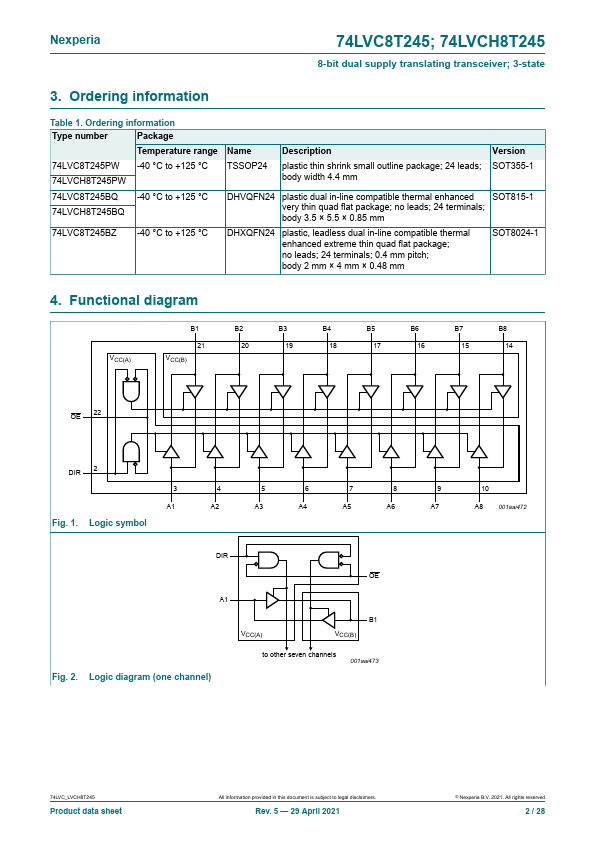
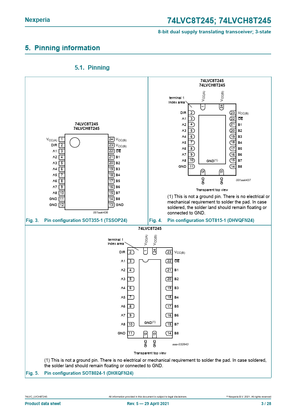
The 74LVC8T245; 74LVCH8T245 are 8-bit dual supply translating transceivers with 3-state outputs that enable bidirectional level translation. They feature two data input-output ports (pins An and Bn), a direction control input (DIR), an output enable input (OE) and dual supply pins (VCC(A) and VCC(B)). Both VCC(A) and VCC(B) can be supplied at any voltage between 1.2 V and 5.5 V making the device suitable for translating between any of the low voltage nodes (1.2 V, 1.5 V, 1.8 V, 2.5 V, 3.3 V and 5.0 V). Pins An, OE and DIR are referenced to VCC(A) and pins Bn are referenced to VCC(B).
 74LVCH8T245 Datasheet