Datasheet Details
| Part number | 74HCT107 |
|---|---|
| Manufacturer | Nexperia |
| File Size | 262.00 KB |
| Description | Dual JK flip-flop |
| Datasheet |
 74HCT107 Datasheet 74HCT107 Datasheet
|
|
|
Download the 74HCT107 datasheet PDF. This datasheet also covers the 74HC107 variant, as both devices belong to the same dual jk flip-flop family and are provided as variant models within a single manufacturer datasheet.
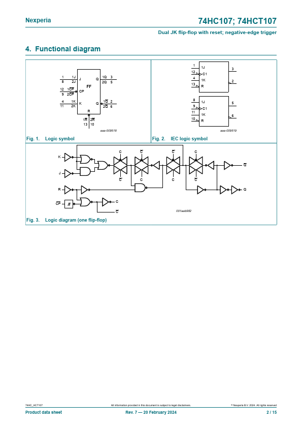
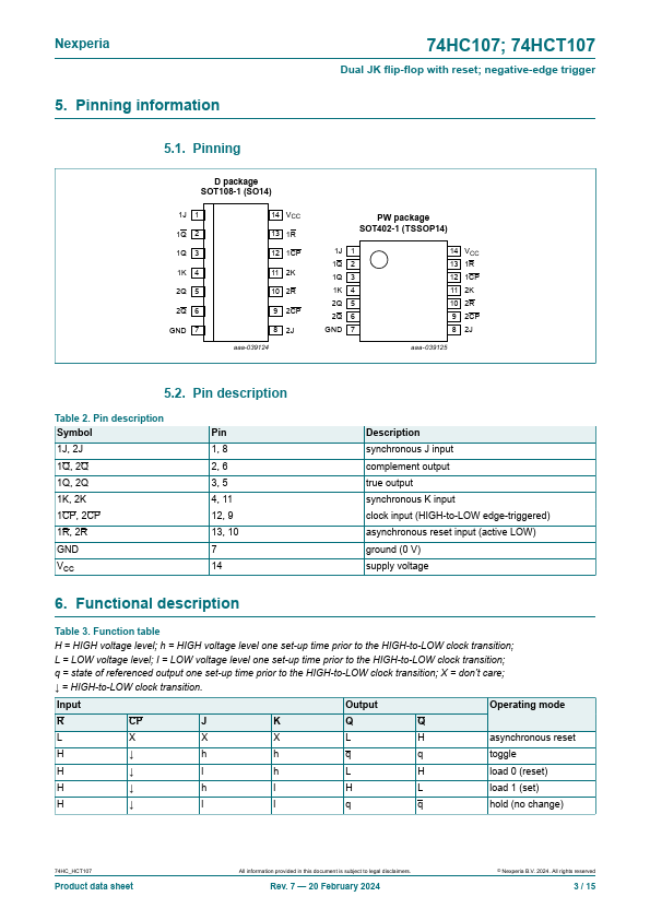
The 74HC107; 74HCT107 is a dual negative edge triggered JK flip-flop featuring individual J and K inputs, clock (CP) and reset (R) inputs and complementary Q and Q outputs.
The reset is an asynchronous active LOW input and operates independently of the clock input.
| Part number | 74HCT107 |
|---|---|
| Manufacturer | Nexperia |
| File Size | 262.00 KB |
| Description | Dual JK flip-flop |
| Datasheet |
74HCT107 Datasheet
|
|
|
|
| Part Number | Description | Manufacturer |
|---|---|---|
| 74HCT107 | Dual JK flip-flop | Philips |
| 74HCT10 | Triple 3-input NAND gate | Philips |
| 74HCT109 | Dual JK flip-flop | Philips |
| 74HCT11 | Triple 3-input AND gate | Philips |
| 74HCT11 | Triple 3-input AND gate | NXP |
| Part Number | Description |
|---|---|
| 74HCT107-Q100 | Dual JK flip-flop |
| 74HCT107D | Dual JK flip-flop |
| 74HCT10 | Triple 3-input NAND gate |
| 74HCT10-Q100 | Triple 3-input NAND gate |
| 74HCT109 | Dual JK flip-flop |
The following content is an automatically extracted verbatim text from the original manufacturer datasheet and is provided for reference purposes only.