Description
4 5 Product Family Comparison 5 6 Product Feature Overview 7 7 Pin Configuration and Functions 8 8 Specifications 10
8.1 Absolute Maximum Ratings 10 8.2 Handling Ratings 10 8.3 Recommended Operating Conditions 11 8.4 Thermal Information 11 8.5 Electrical Characteristics 11 8.6 Timing Characteristics 13 8.7 PMBUS/SMBUS/IC Timing2 14 8.8 Timing Requirements 14 8.9 Power On Reset (POR) / Brown Out Detect
(BOD) 16 8.10 Typical Clock Gating Power Savings 17 8.11 Typical Characteristics 18 9
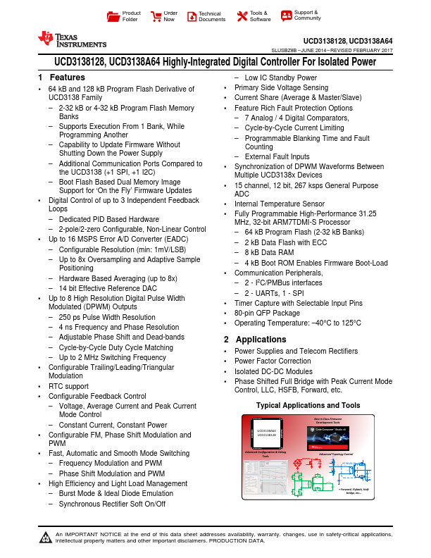
Features
- 1 64 kB and 128 kB Program Flash Derivative of UCD3138 Family.
- 2-32 kB or 4-32 kB Program Flash Memory Banks.
- Supports Execution From 1 Bank, While Programming Another.
- Capability to Update Firmware Without Shutting Down the Power Supply.
- Additional Communication Ports Compared to the UCD3138 (+1 SPI, +1 I2C).
- Boot Flash Based Dual Memory Image Support for ‘On the Fly’ Firmware Updates.
- Digital Control of up to 3 Independent Feedback.
 UCD3138128-etcTI.pdf