Datasheet Details
| Part number | SN74AUC34 |
|---|---|
| Manufacturer | Texas Instruments |
| File Size | 811.31 KB |
| Description | HEX BUFFER GATE |
| Datasheet |
 SN74AUC34 Datasheet SN74AUC34 Datasheet
|
|
|
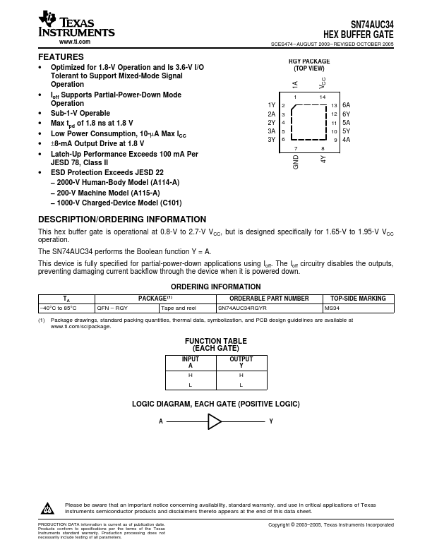
This hex buffer gate is operational at 0.8-V to 2.7-V VCC, but is designed specifically for 1.65-V to 1.95-V VCC operation.
The SN74AUC34 performs the Boolean function Y = A.
This device is fully specified for partial-power-down applications using Ioff.
| Part number | SN74AUC34 |
|---|---|
| Manufacturer | Texas Instruments |
| File Size | 811.31 KB |
| Description | HEX BUFFER GATE |
| Datasheet |
SN74AUC34 Datasheet
|
|
|
|
| Part Number | Description | Manufacturer |
|---|---|---|
| SN74101 | AND-OR Gate | ETC |
| SN74102 | AND Gate | ETC |
| SN74103 | Dual J-K Flip-Flop | ETC |
| SN74106 | Dual J-K Flip-Flop | ETC |
| SN74108 | Dual J-K Flip Flop | ETC |
| Part Number | Description |
|---|---|
| SN74AUC32 | QUADRUPLE 2-INPUT POSITIVE-OR GATE |
| SN74AUC32244 | 32-BIT BUFFER/DRIVER |
| SN74AUC32245 | 32-BIT BUS TRANSCEIVER |
| SN74AUC32374 | 32-BIT EDGE-TRIGGERED D-TYPE FLIP-FLOP |
| SN74AUC00 | QUADRUPLE 2-INPUT POSITIVE-NAND GATE |
The following content is an automatically extracted verbatim text from the original manufacturer datasheet and is provided for reference purposes only.