Datasheet4U Logo Datasheet4U.com

SN74AHCT367 Hex Buffer and Line Driver

SN74AHCT367 Description

Product Folder Sample & Buy Technical Documents Tools & Software Support & Community SN74AHCT367 SCLS418H * JUNE 1998 * REVISED D.
The SN74AHCT367 device is designed specifically to improve both the performance and density of 3-state memory address drivers, clock drivers, and bus-.

SN74AHCT367 Features

* 1 Inputs are TTL-Voltage Compatible
* True Outputs
* Latch-Up Performance Exceeds 100 mA Per JESD 78, Class II
* ESD Protection Exceeds JESD 22
* 2000-V Human-Body Model
* 200-V Machine Model

SN74AHCT367 Applications

* Telecom Infrastructure
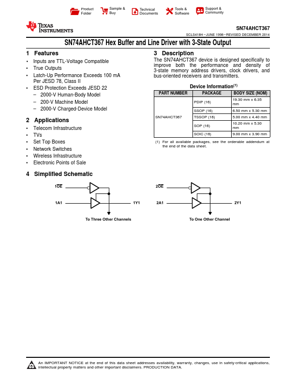
* TVs
* Set Top Boxes
* Network Switches
* Wireless Infrastructure

📥 Download Datasheet

Preview of SN74AHCT367 PDF
datasheet Preview Page 2 datasheet Preview Page 3

📁 Related Datasheet

  • SN74101 - AND-OR Gate (ETC)
  • SN74102 - AND Gate (ETC)
  • SN74103 - Dual J-K Flip-Flop (ETC)
  • SN74106 - Dual J-K Flip-Flop (ETC)
  • SN74108 - Dual J-K Flip Flop (ETC)
  • SN7411 - Triple 3-Input AND (ETC)
  • SN74120 - Dual Pulse Synchronizers / Drivers (Texas Instruments Inc)
  • SN74124 - Dual Voltage Controlled Oscillators (ETC)

📌 All Tags

Texas Instruments SN74AHCT367-like datasheet