Datasheet Details
| Part number | LMK1D1216 |
|---|---|
| Manufacturer | Texas Instruments |
| File Size | 2.79 MB |
| Description | Low Additive Jitter LVDS Buffer |
| Datasheet |
 LMK1D1216 Datasheet LMK1D1216 Datasheet
|
|
|
Download the LMK1D1216 datasheet PDF. This datasheet also covers the LMK1D1212 variant, as both devices belong to the same low additive jitter lvds buffer family and are provided as variant models within a single manufacturer datasheet.
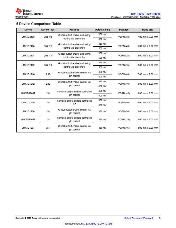
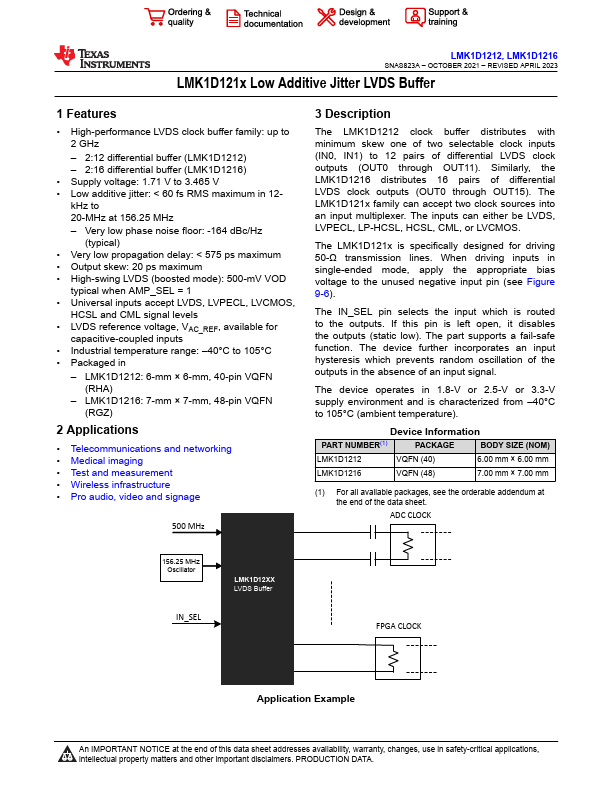
The LMK1D1212 clock buffer distributes with minimum skew one of two selectable clock inputs (IN0, IN1) to 12 pairs of differential LVDS clock outputs (OUT0 through OUT11).
Similarly, the LMK1D1216 distributes 16 pairs of differential LVDS clock outputs (OUT0 through OUT15).
| Part number | LMK1D1216 |
|---|---|
| Manufacturer | Texas Instruments |
| File Size | 2.79 MB |
| Description | Low Additive Jitter LVDS Buffer |
| Datasheet |
LMK1D1216 Datasheet
|
|
|
|
| Part Number | Description | Manufacturer |
|---|---|---|
| LMK104DNEFWU-AKA | LCD | TOPWAY |
| LMK105 | MULTILAYER CERAMIC CAPACITORS | Taiyo Yuden |
| LMK01000 | (LMK01000 - LMK01020) 1.6 GHz High Performance Clock Buffer | National Semiconductor |
| LMK01010 | (LMK01000 - LMK01020) 1.6 GHz High Performance Clock Buffer | National Semiconductor |
| LMK01020 | (LMK01000 - LMK01020) 1.6 GHz High Performance Clock Buffer | National Semiconductor |
| Part Number | Description |
|---|---|
| LMK1D1212 | Low Additive Jitter LVDS Buffer |
| LMK1C1102 | LVCMOS Clock Buffer |
| LMK1C1103 | LVCMOS Clock Buffer |
| LMK1C1104 | LVCMOS Clock Buffer |
| LMK00101 | Ultra-low Jitter LVCMOS Fanout Buffer/Level Translator |
The following content is an automatically extracted verbatim text from the original manufacturer datasheet and is provided for reference purposes only.