Datasheet Details
| Part number | CDC857-2 |
|---|---|
| Manufacturer | Texas Instruments |
| File Size | 155.46 KB |
| Description | 2.5-/3.3-V PHASE-LOCK LOOP CLOCK DRIVERS |
| Datasheet |
 CDC857-2 Datasheet CDC857-2 Datasheet
|
|
|
| Part number | CDC857-2 |
|---|---|
| Manufacturer | Texas Instruments |
| File Size | 155.46 KB |
| Description | 2.5-/3.3-V PHASE-LOCK LOOP CLOCK DRIVERS |
| Datasheet |
CDC857-2 Datasheet
|
|
|
|
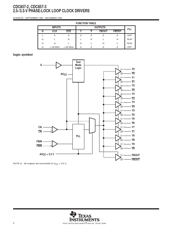
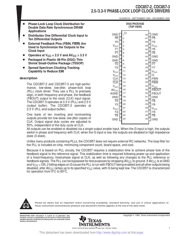
VCC 11 VCC 12 CLK 13 38 VCC 37 G 36 FBIN The CDC857-2 and CDC857-3 are high-performance, low-skew, low-jitter, phase-lock loop (PLL) clock driver.They use a PLL to precisely align, in both frequency and phase, the feedback (FBOUT) output to the clock (CLK) input signal.The CDC857-3 operates at 3.3 V (PLL) and 2.5 V (output buffer).The CDC857-2 operates at 2.5 V (PLL and output buffer).One bank of ten inverting and noninverting outputs provide ten low-skew, low-jitter copies of CLK.Output
📁 Similar Datasheet