Datasheet Details
| Part number | CDC3S04 |
|---|---|
| Manufacturer | Texas Instruments |
| File Size | 1.60 MB |
| Description | Quad Sine-Wave Clock Buffer |
| Datasheet |
 CDC3S04 Datasheet CDC3S04 Datasheet
|
|
|
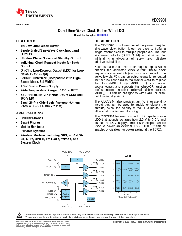
The CDC3S04 is a four-channel low-power low-jitter sine-wave clock buffer.
It can be used to buffer a single master clock to multiple peripherals.
CLK4) are designed for minimal channel-to-channel skew and ultralow additive output jitter.
| Part number | CDC3S04 |
|---|---|
| Manufacturer | Texas Instruments |
| File Size | 1.60 MB |
| Description | Quad Sine-Wave Clock Buffer |
| Datasheet |
CDC3S04 Datasheet
|
|
|
|
| Part Number | Description | Manufacturer |
|---|---|---|
| CDC3207G-C | Automotive Controller | Micronas |
| CDC3207G-C3 | Automotive Controller | Micronas |
| CDC3257G-C2 | Automotive Controller | Micronas |
| CDC-Z137 | FM / AM CD Player | Aiwa |
| CDC1607F-E | Automotive Controller Specification | Micronas |
| Part Number | Description |
|---|---|
| CDC318A | 1-Line To 18-Line Clock Driver |
| CDC319 | 1-Line To 10-Line Clock Driver |
| CDC328A | 1-Line To 6-Line Clock Driver |
| CDC329A | 1-Line To 6-Line Clock Driver |
| CDC337 | Clock Driver |
The following content is an automatically extracted verbatim text from the original manufacturer datasheet and is provided for reference purposes only.