Click to expand full text
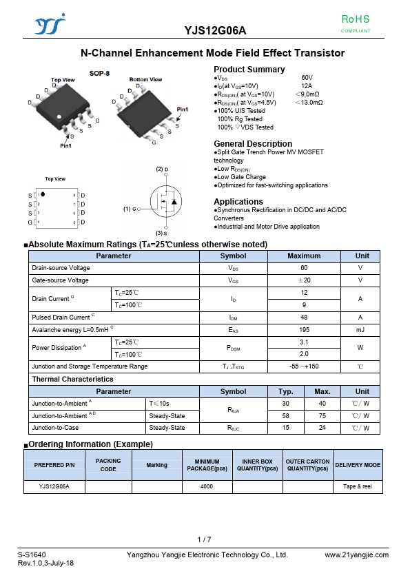
YJS12G06A
RoHS
COMPLIANT
N-Channel Enhancement Mode Field Effect Transistor
Product Summary
●VDS ●ID(at VGS=10V) ●RDS(ON)( at VGS=10V) ●RDS(ON)( at VGS=4.5V) ●100% UIS Tested
100% Rg Tested 100% ▽VDS Tested
60V 12A <9.0mΩ <13.0mΩ
Top View
General Description
●Split Gate Trench Power MV MOSFET technology ●Low RDS(ON) ●Low Gate Charge ●Optimized for fast-switching applications
Applications
●Synchronus Rectification in DC/DC and AC/DC Converters ●Industrial and Motor Drive application
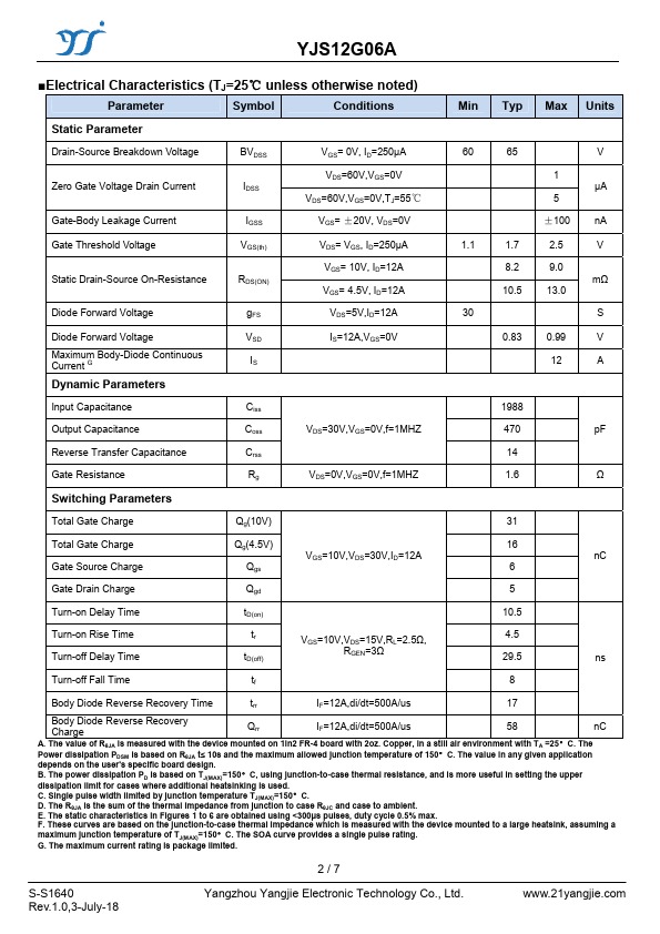
■Absolute Maximum Ratings (TA=25℃unless otherwise noted)
Parameter
Symbol
Drain-source Voltage
VDS
Gate-source Voltage
VGS
Drain Current G
TC=25℃
ID
TC=100℃
Pulsed Drain Current C
IDM
Avalanche energy L=0.
 YJS12G06A Datasheet