Click to expand full text
DS183 (v1.29) March 23, 2021
Virtex‐7 T and XT FPGAs Data Sheet: DC and AC Switching Characteristics
Product Specification
Introduction
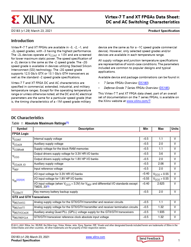
Virtex®-7 T and XT FPGAs are available in -3, -2, -1, and -2L speed grades, with -3 having the highest performance. The -2L devices operate at VCCINT = 1.0V and are screened for lower maximum static power. The speed specification of a -2L device is the same as the -2 speed grade. The -2G speed grade is available in devices utilizing Stacked Silicon Interconnect (SSI) technology. The -2G speed grade supports 12.5 Gb/s GTX or 13.1 Gb/s GTH transceivers as well as the standard -2 speed grade specifications. Virtex-7 T and XT FPGA DC and AC characteristics are specified in commercial, extended, industrial, and military temperature ranges.
 XC7VX330T Datasheet