Description
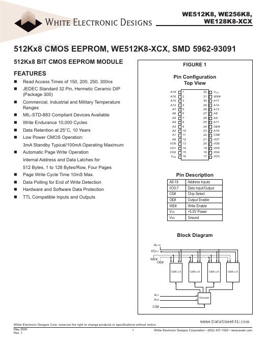
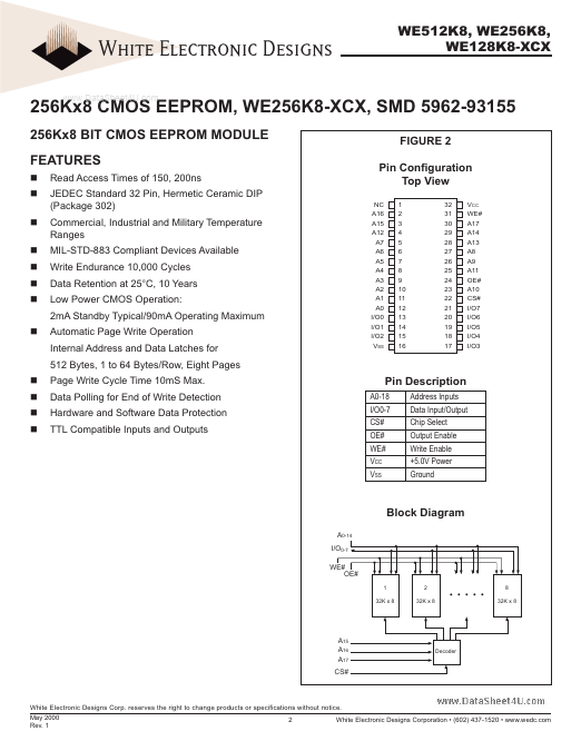
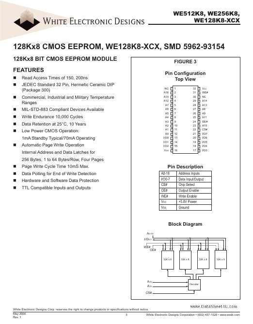
A0-18 I/O0-7 CS# OE# WE# VCC VSS Address Inputs Data Input/Output Chip Select Output Enable Write Enable +5.0V Power Ground
Block Diagram
A0-16 I/O0-7 WE# OE#
128K x 8 128K x 8 128K x 8 128K x 8
A17 A18 CS#
Decoder
White Electronic Designs Corp.reserves the right to change products or specifications without notice.May 2000 Rev.1 1 White Electronic Designs Corporation
(602) 437-1520
www.wedc.com
White Electronic Designs
www.DataSheet4U.com
WE512K8, WE256K8, WE128K8-XCX
Features
- Read Access Times of 150, 200, 250, 300ns JEDEC Standard 32 Pin, Hermetic Ceramic DIP (Package 300) Commercial, Industrial and Military Temperature Ranges MIL-STD-883 Compliant Devices Available Write Endurance 10,000 Cycles Data Retention at 25°C, 10 Years Low Power CMOS Operation: 3mA Standby Typical/100mA Operating Maximum Automatic Page Write Operation Internal Address and Data Latches for 512 Bytes, 1 to 128 Bytes/Row, Four Pages Page Write Cycle Time 10mS Max. Data Polling for End of Write.
 WE256K8_WhiteElectronicDesignsCorporation.pdf