The following content is an automatically extracted verbatim text
from the original manufacturer datasheet and is provided for reference purposes only.
View original datasheet text
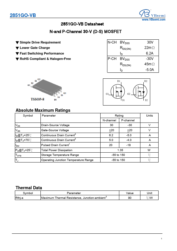
2851GO-VB
2851GO-VB Datasheet N-and P-Channel 30-V (D-S) MOSFET
▼ Simple Drive Requirement ▼ Lower Gate Charge ▼ Fast Switching Performance ▼ RoHS Compliant & Halogen-Free
N-CH P-CH
BVDSS RDS(ON) ID BVDSS RDS(ON) ID
D1
www.VBsemi.com
30V 22mΩ 6.2A -30V 45mΩ -5.0A
D2
Absolute Maximum Ratings
Symbol
Parameter
VDS VGS ID@TA=25℃ ID@TA=70℃ IDM PD@TA=25℃ TSTG TJ
Drain-Source Voltage
Gate-Source Voltage Continuous Drain Current3 Continuous Drain Current3 Pulsed Drain Current1 Total Power Dissipation Storage Temperature Range Operating Junction Temperature Range
G1
G2
S1
Rating
N-channel P-channel
30
-30
+20
+20
6.2
-5.0
5.0
-4.0
20
-18
1.
 2851GO Datasheet