Datasheet Details
| Part number | CHA2110-98F |
|---|---|
| Manufacturer | United Monolithic Semiconductors |
| File Size | 673.10 KB |
| Description | 7-12GHz LNA |
| Datasheet |
 CHA2110-98F Datasheet CHA2110-98F Datasheet
|
|
|
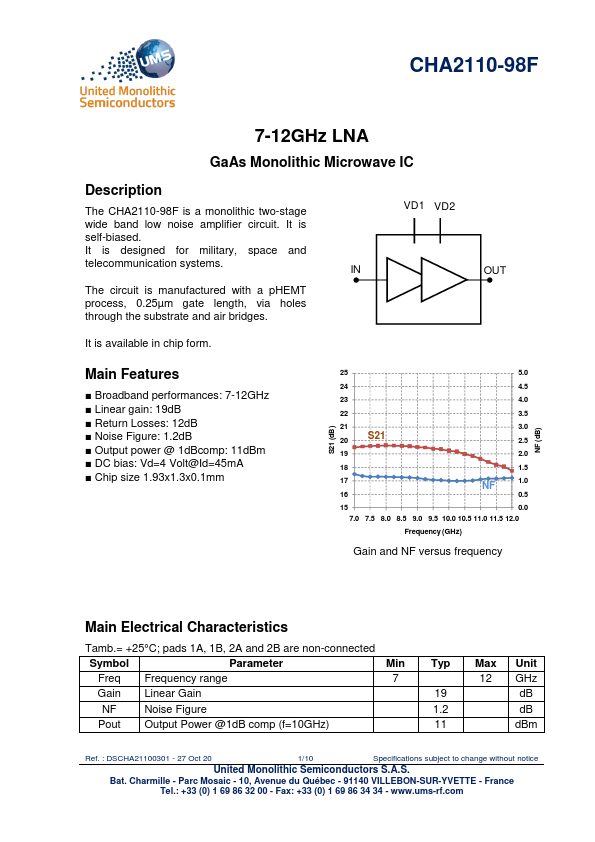
The CHA2110-98F is a monolithic two-stage wide band low noise amplifier circuit.
It is self-biased.
telecommunication systems.
| Part number | CHA2110-98F |
|---|---|
| Manufacturer | United Monolithic Semiconductors |
| File Size | 673.10 KB |
| Description | 7-12GHz LNA |
| Datasheet |
CHA2110-98F Datasheet
|
|
|
|
| Part Number | Description | Manufacturer |
|---|---|---|
| CHA-20NF | (CHA-20xx) Coaxial Attenuators | Component General |
| CHA-20NM | (CHA-20xx) Coaxial Attenuators | Component General |
| CHA-20NMF | (CHA-20xx) Coaxial Attenuators | Component General |
| CHA-20SF | (CHA-20xx) Coaxial Attenuators | Component General |
| CHA-20SM | (CHA-20xx) Coaxial Attenuators | Component General |
| Part Number | Description |
|---|---|
| CHA2110-QDG | GaAs Monolithic Microwave |
| CHA2157 | 55-60GHz Low Noise / Medium Power Amplifier |
| CHA2157-99F | Medium Power Amplifier |
| CHA2159 | 55-65GHz Low Noise / Medium Power Amplifier |
| CHA2159-99F | Low Noise / Medium Power Amplifier |
The following content is an automatically extracted verbatim text from the original manufacturer datasheet and is provided for reference purposes only.