The following content is an automatically extracted verbatim text
from the original manufacturer datasheet and is provided for reference purposes only.
View original datasheet text
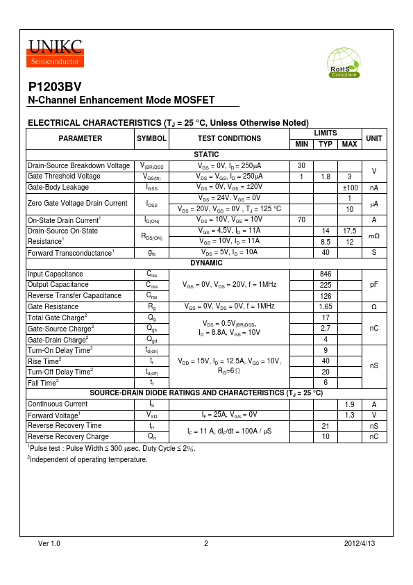
P1203BV
N-Channel Enhancement Mode MOSFET
PRODUCT SUMMARY
V(BR)DSS 30V RDS(ON) 12mΩ @VGS = 10V ID 11A
SOP- 08
ABSOLUTE MAXIMUM RATINGS (TA = 25 ° C Unless Otherwise Noted)
PARAMETERS/TEST CONDITIONS Drain-Source Voltage Gate-Source Voltage Continuous Drain Current2 Pulsed Drain Current Avalanche Current Avalanche Energy Power Dissipation
1,2
http://www.DataSheet4U.net/
SYMBOL VDS VGS
LIMITS 30 ±20 11 7 40 28 40 2.5 1 -55 to 150
UNITS V
TA = 25 ° C TA = 100 ° C
ID IDM IAS
A
L = 0.1mH TA = 25 ° C TA = 100 ° C
EAS PD TJ, TSTG
mJ W ° C
Operating Junction & Storage Temperature Range
THERMAL RESISTANCE RATINGS
THERMAL RESISTANCE Junction-to-Case Junction-to-Ambient
1 2
SYMBOL RqJC RqJA
TYPICAL
MAXIMUM 25 50
UNITS ° C/W
Pulse width limited by maximum junction temperature.
 P1203BV Datasheet