Datasheet Details
| Part number | TC7WB67CL8X |
|---|---|
| Manufacturer | Toshiba Electronic Devices & Storage |
| File Size | 278.70 KB |
| Description | Dual SPST Bus Switch |
| Datasheet |
 TC7WB67CL8X Datasheet TC7WB67CL8X Datasheet
|
|
|
Download the TC7WB67CL8X datasheet PDF (TC7WB66CFK included). The manufacturer datasheet provides complete specifications, pinout details, electrical characteristics, and typical applications for dual spst bus switch.
2.
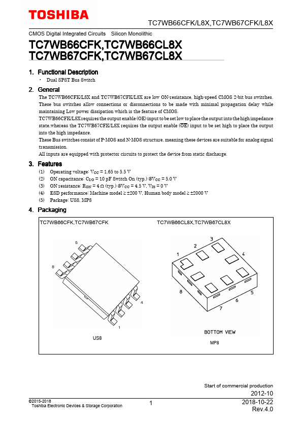
The TC7WB66CFK/L8X and TC7WB67CFK/L8X are low ON-resistance, high-speed CMOS 2-bit bus switches.
| Part number | TC7WB67CL8X |
|---|---|
| Manufacturer | Toshiba Electronic Devices & Storage |
| File Size | 278.70 KB |
| Description | Dual SPST Bus Switch |
| Datasheet |
TC7WB67CL8X Datasheet
|
|
|
|