The following content is an automatically extracted verbatim text
from the original manufacturer datasheet and is provided for reference purposes only.
View original datasheet text
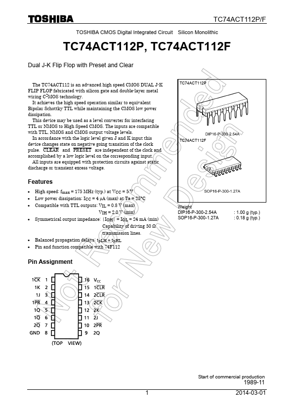
TC74ACT112P/F
TOSHIBA CMOS Digital Integrated Circuit Silicon Monolithic
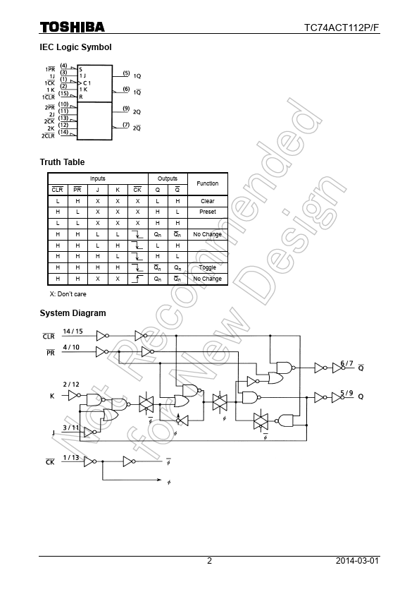
TC74ACT112P, TC74ACT112F
Dual J-K Flip Flop with Preset and Clear
The TC74ACT112 is an advanced high speed CMOS DUAL J-K FLIP FLOP fabricated with silicon gate and double-layer metal wiring C2MOS technology.
It achieves the high speed operation similar to equivalent Bipolar Schottky TTL while maintaining the CMOS low power dissipation.
This device may be used as a level converter for interfacing TTL or NMOS to High Speed CMOS. The inputs are compatible with TTL, NMOS and CMOS output voltage levels.
In accordance with the logic level given J and K input this device changes state on negative going transition of the clock pulse.
 TC74ACT112P Datasheet