Datasheet Details
| Part number | TC518129BFWL-10V |
|---|---|
| Manufacturer | Toshiba |
| File Size | 473.01 KB |
| Description | SILICON GATE CMOS PSEUDO STATIC RAM |
| Datasheet |
 TC518129BFWL-10V Datasheet TC518129BFWL-10V Datasheet
|
|
|
Download the TC518129BFWL-10V datasheet PDF. This datasheet also covers the TC518129BPL-70V variant, as both devices belong to the same silicon gate cmos pseudo static ram family and are provided as variant models within a single manufacturer datasheet.
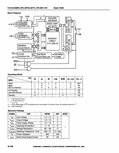
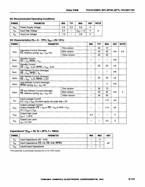
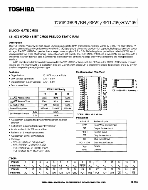
The TC518129B-V is a 1M bit high speed CMOS pseudo static RAM organized as 131,072 words by 8 bits.
The TC518129B-V utilizes a one transistor dynamic memory cell with CMOS peripheral circuitry to provide high capacity, high speed and low power storage.
| Part number | TC518129BFWL-10V |
|---|---|
| Manufacturer | Toshiba |
| File Size | 473.01 KB |
| Description | SILICON GATE CMOS PSEUDO STATIC RAM |
| Datasheet |
TC518129BFWL-10V Datasheet
|
|
|
|
| Part Number | Description | Manufacturer |
|---|---|---|
| TC51 | 1uA Voltage Detector | Microchip |
| TC510 | Precision Analog Front Ends | Microchip |
| TC510 | (TC5xx) PRECISION ANALOG FRONT ENDS | TelCom Semiconductor |
| TC511402 | 1048576 x 4 BIT DYNAMIC RAM | Toshiba Semiconductor |
| TC511402AJ-60 | DRAM | Toshiba Semiconductor |
| Part Number | Description |
|---|---|
| TC518129BFWL-10 | CMOS Pseudo Static RAM |
| TC518129BFWL-10L | CMOS Pseudo Static RAM |
| TC518129BFWL-70 | CMOS Pseudo Static RAM |
| TC518129BFWL-70L | CMOS Pseudo Static RAM |
| TC518129BFWL-70V | SILICON GATE CMOS PSEUDO STATIC RAM |
The following content is an automatically extracted verbatim text from the original manufacturer datasheet and is provided for reference purposes only.