Description
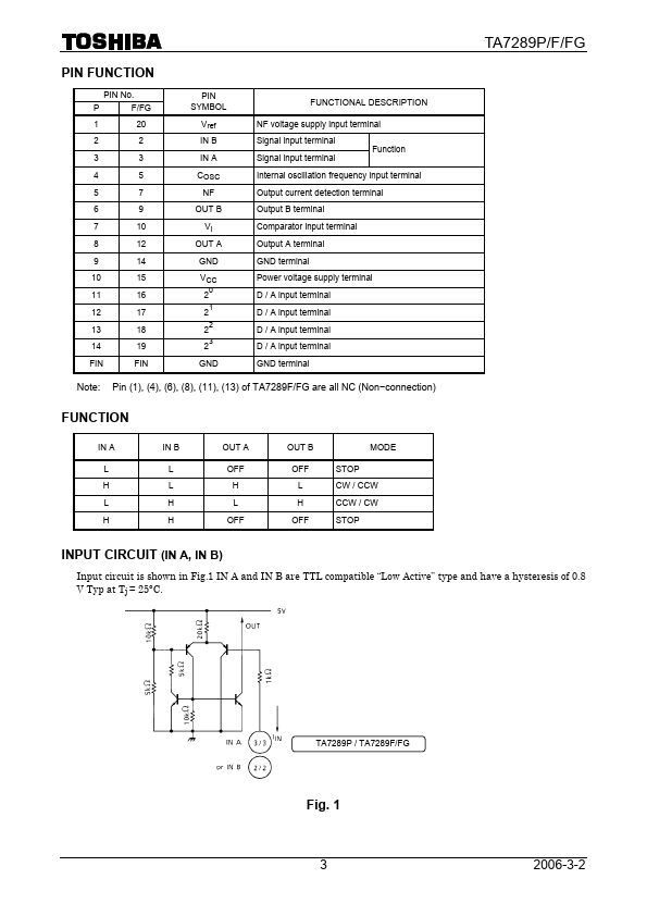
NF voltage supply input terminal
Signal input terminal Signal input terminal
Function
Internal oscillation frequency input terminal
Output current detection terminal
Output B terminal
Comparator input terminal
Output A terminal
GND terminal
Power voltage supply terminal
D / A input terminal
D / A input terminal
D / A input terminal
D / A input terminal
GND terminal
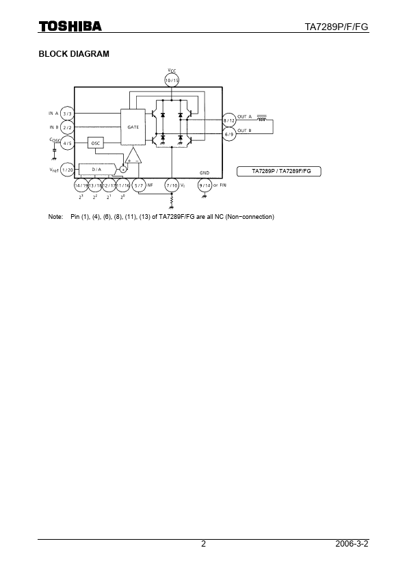
Note: Pin (1), (4), (6), (8), (11), (13) of TA7289F/FG are all NC (Non
connection)
FUNCTION
IN A
IN B
OU
Features
- z Wide Range of Operating Voltage : VCC (opr. ) Min. = 6~27 V
z High Current Capability: IO Max = 1.5 A (PEAK) z LS.
- TTL Compatible Control Inputs (IN A, IN B) z Few External Components Required. z Build.
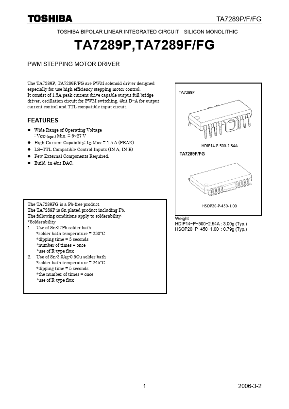
- in 4bit DAC. TA7289F/FG
The TA7289FG is a Pb-free product. The TA7289P is Sn plated product including Pb. The following conditions apply to solderability:.
- Solderability 1. Use of Sn-37Pb solder bath.
- solder bath temperature = 230°C.
- dipping time = 5 seconds.
- numb.
 TA7289F_ToshibaSemiconductor.pdf