The following content is an automatically extracted verbatim text
from the original manufacturer datasheet and is provided for reference purposes only.
View original datasheet text
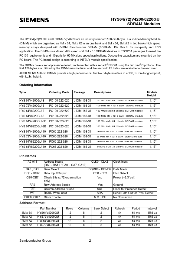
3.3V 4M x 64/72-Bit 1 BANK SDRAM Module 3.3V 8M x 64/72-Bit 2 BANK SDRAM Module
HYS64(72)V4200GU HYS64(72)V8220GU
PC66 & PC100 168 pin unbuffered DIMM Modules
•
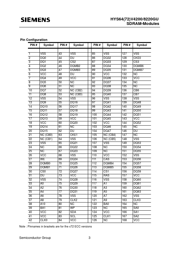
168 Pin unbuffered 8 Byte Dual-In-Line SDRAM Modules for PC main memory applications One bank 4M x 64, 4Mx72 and two bank 8M x 64, 8M x 72 organisation Optimized for byte-write non-parity and ECC applications JEDEC standard Synchronous DRAMs (SDRAM) Fully PC board layout compatible to INTEL’s Rev. 1.0 module specification SDRAM Performance:
-8 fCK tAC Clock frequency (max.) Clock access time 100 6 -8B 100 6 -10 66 8 Units MHz ns
• • • • •
•
Programmed Latencies :
Product Speed -8 -8B -10 PC100 PC100 PC66 CL 2 3 2 tRCD 2 2 2 tRP 2 3 2
• •
Single +3.3V(± 0.
 HYS72V4200GU-8 Datasheet