Description
EDO-DRAM (access time 50 ns) EDO-DRAM (access time 60 ns) EDO-DRAM (access time 70 ns) Low Power EDO-DRAM (access time 50 ns) Low Power EDO-DRAM (access time 60 ns) Low Power EDO-DRAM (access time 70 ns)
Semiconductor Group
2
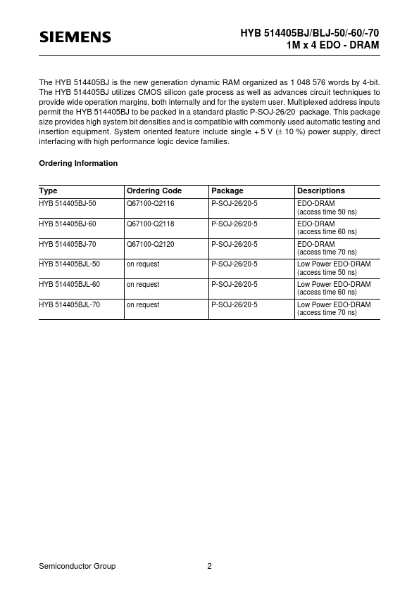
HYB 514405BJ/BJL-50/-60/-70 1M x 4 EDO - DRAM
Pin Configuration (top view)
P-SOJ-26/20-5
Pin Names A0-A9 RAS CAS WE OE I/O1 - I/O4 Address Input Row Address Strobe Column Address Strobe Read/Write Input Output Enable Data Input/Output Power Supply (+ 5 V) Ground (0 V
Features
- 5 10 10.
- ns ns ns ns ns
CAS-before-RAS Counter Test Cycle
CAS precharge time (CASbefore-RAS counter test cycle)
tCPT
35.
- 40.
- 40.
- ns
Test Mode
Write command setup time Write command hold time
tWTS tWTH
10 10.
- 10 10.
- 10 10.
- ns ns
Capacitance TA = 0 to 70 ˚C; VCC = 5 V ± 10 %; f = 1 MHz Parameter Input capacitance (A0 to A9) Input capacitance (RAS.

 HYB-5144.pdf