Description
3.3V 50ns 256 K x 16 DRAM 3.3V 60 ns 256 K x 16 DRAM 3.3V 70 ns 256 K x 16 DRAM 3.3V 50 ns 256 K x 16 DRAM 3.3V 60 ns 256 K x 16 DRAM 3.3V 70 ns 256 K x 16 DRAM
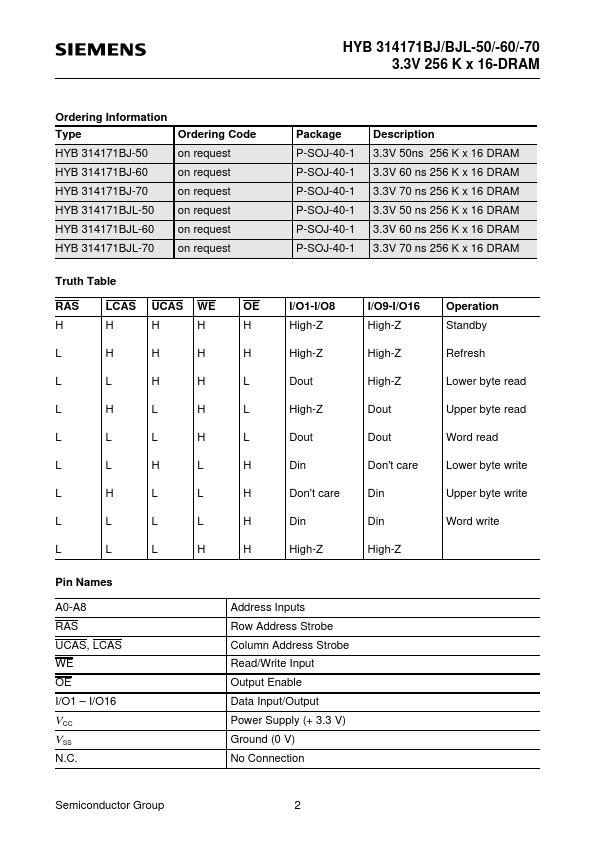
Pin Names A0-A8 RAS UCAS, LCAS WE OE I/O1
I/O16 Address Inputs Row Address Strobe Column Address Strobe Read/Write Input Output Enable Data Input/Output Power Supply (+ 3.3 V) Ground (0 V) No Connection
VCC VSS
N.C.Semiconductor Group
2
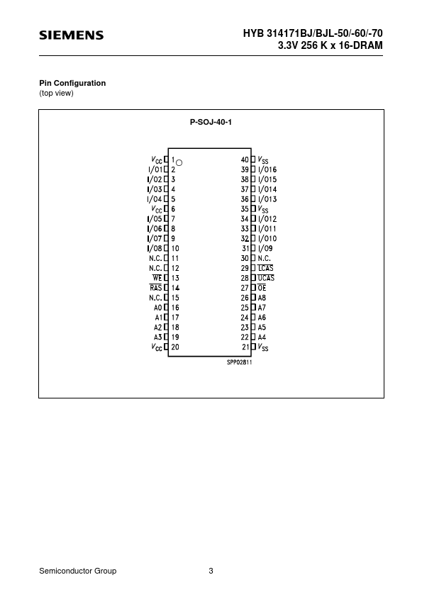
HYB 314171BJ/BJL-50/-60/-70 3.3V 256 K x 16-DRAM
Pin Configuration (top view)
P-SOJ-
Features
- include Self Refresh (LVersion), single + 3.3 V (± 0.3 V) power supply, direct interfacing with high performance logic device families. Semiconductor Group
1
7.96
HYB 314171BJ/BJL-50/-60/-70 3.3V 256 K x 16-DRAM
Ordering Information Type HYB 314171BJ-50 HYB 314171BJ-60 HYB 314171BJ-70 HYB 314171BJL-50 HYB 314171BJL-60 HYB 314171BJL-70 Truth Table RAS H L L L L L L L L LCAS H H L H L L H L L UCAS H H H L L H L L L WE H H H H H L L L H OE H H L L L H H H H I/O1-I/O8 High-Z High-Z Dout High-Z.
 HYB-314-171.pdf